ZHCSF93E December 2015 – August 2020 LMR23630
PRODUCTION DATA
- 1 特性
- 2 应用
- 3 说明
- 4 Revision History
- 5 Device Comparison Table
- 6 Pin Configuration and Functions
- 7 Specifications
-
8 Detailed Description
- 8.1 Overview
- 8.2 Functional Block Diagram
- 8.3
Feature Description
- 8.3.1 Fixed Frequency Peak Current Mode Control
- 8.3.2 Adjustable Frequency
- 8.3.3 Adjustable Output Voltage
- 8.3.4 Enable/Sync
- 8.3.5 VCC, UVLO
- 8.3.6 Minimum ON-time, Minimum OFF-time and Frequency Foldback at Dropout Conditions
- 8.3.7 Power Good (PGOOD)
- 8.3.8 Internal Compensation and CFF
- 8.3.9 Bootstrap Voltage (BOOT)
- 8.3.10 Overcurrent and Short-Circuit Protection
- 8.3.11 Thermal Shutdown
- 8.4 Device Functional Modes
-
9 Application and Implementation
- 9.1 Application Information
- 9.2
Typical Applications
- 9.2.1 Design Requirements
- 9.2.2
Detailed Design Procedure
- 9.2.2.1 Custom Design With WEBENCH® Tools
- 9.2.2.2 Output Voltage Setpoint
- 9.2.2.3 Switching Frequency
- 9.2.2.4 Inductor Selection
- 9.2.2.5 Output Capacitor Selection
- 9.2.2.6 Feed-Forward Capacitor
- 9.2.2.7 Input Capacitor Selection
- 9.2.2.8 Bootstrap Capacitor Selection
- 9.2.2.9 VCC Capacitor Selection
- 9.2.2.10 Undervoltage Lockout Setpoint
- 9.2.3 Application Curves
- 10Power Supply Recommendations
- 11Layout
- 12Device and Documentation Support
- 13Mechanical, Packaging, and Orderable Information
封装选项
请参考 PDF 数据表获取器件具体的封装图。
机械数据 (封装 | 引脚)
- DRR|12
- DDA|8
散热焊盘机械数据 (封装 | 引脚)
订购信息
8.3.7 Power Good (PGOOD)
The power-good version of LMR23630 has a built in power-good flag shown on PGOOD pin to indicate whether the output voltage is within its regulation level. The PGOOD signal can be used for start-up sequencing of multiple rails or fault protection. The PGOOD pin is an open-drain output that requires a pullup resistor to an appropriate DC voltage. Voltage detected by the PGOOD pin must never exceed 15 V, and limit the maximum current into this pin to 1 mA. A typical range of pullup resistor value is 10 kΩ to 100 kΩ.
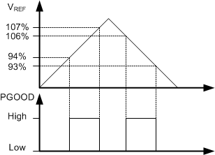
When the FB voltage is within the power-good band, +6% above and –6% below the internal reference voltage VREF typically, the PGOOD switch is turned off, and the PGOOD voltage is as high as the pulled-up voltage. When the FB voltage is outside of the tolerance band, +7% above or –7% below VREF typically, the PGOOD switch is turned on, and the PGOOD pin voltage is pulled low to indicate power bad. A glitch filter prevents false flag operation for short excursions in the output voltage, such as during line and load transients. The values for the various filter and delay times can be found in Section 7.6. Power-good operation can best be understood by reference to Figure 8-9.
 Figure 8-9 Power-Good Flag