ZHCSKF0A October 2019 – June 2022 LMR33610
PRODUCTION DATA
- 1 特性
- 2 应用
- 3 说明
- 4 Revision History
- 5 Device Comparison
- 6 Pin Configuration and Functions
- 7 Specifications
- 8 Detailed Description
-
9 Application and Implementation
- 9.1 Application Information
- 9.2
Typical Application
- 9.2.1 Design Requirements
- 9.2.2
Detailed Design Procedure
- 9.2.2.1 Custom Design With WEBENCH® Tools
- 9.2.2.2 Choosing the Switching Frequency
- 9.2.2.3 Setting the Output Voltage
- 9.2.2.4 Inductor Selection
- 9.2.2.5 Output Capacitor Selection
- 9.2.2.6 Input Capacitor Selection
- 9.2.2.7 CBOOT
- 9.2.2.8 VCC
- 9.2.2.9 CFF Selection
- 9.2.2.10 External UVLO
- 9.2.2.11 Maximum Ambient Temperature
- 9.2.3 Application Curves
- 9.3 What to Do and What Not to Do
- 10Power Supply Recommendations
- 11Layout
- 12Device and Documentation Support
- 13Mechanical, Packaging, and Orderable Information
9.2.3 Application Curves
Unless otherwise specified, the following conditions apply: VIN = 12 V, TA = 25°C. Figure 9-20 shows the circuit with the appropriate BOM from Table 9-3.
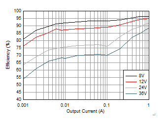
| VOUT = 5 V | 400 kHz | DDA Package |
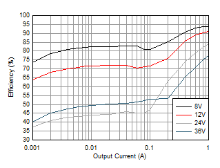
| VOUT = 5 V | 1.4 MHz | DDA Package |
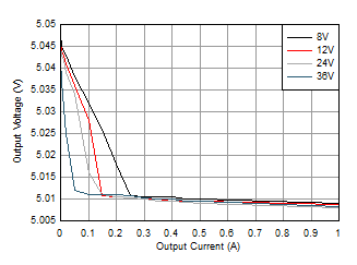
| VOUT = 5 V |
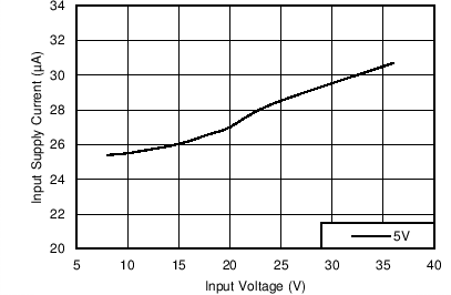
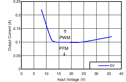
| VOUT = 5 V | IOUT = 0 A | RFBT = 1 MΩ |
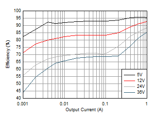
| VOUT = 5 V | ƒSW = 400 kHz |
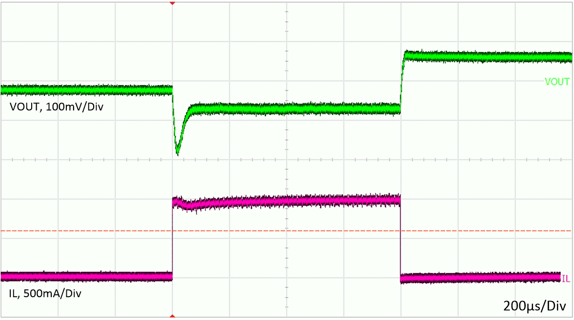
| VIN = 12 V | VOUT = 5 V | |
| tf = tr = 2 µs | IOUT = 0 A to 1 A | |
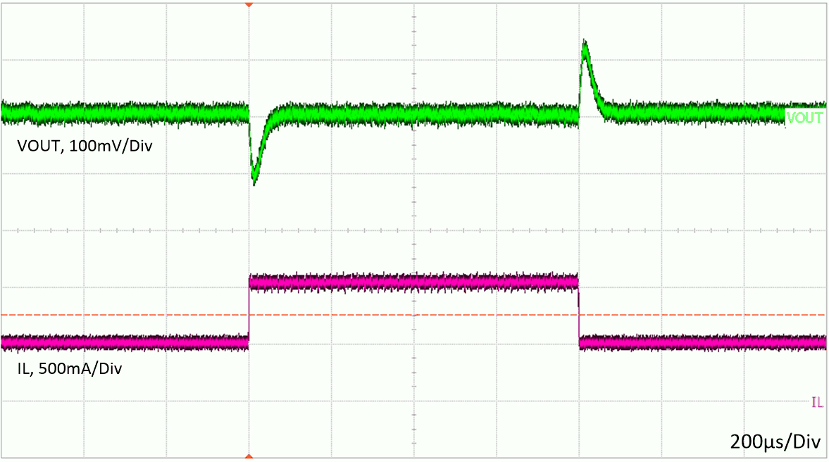
| VIN = 12 V | VOUT = 5 V | |
| tf = tr = 2 µs | IOUT = 0.5 A to 1 A | |
| VOUT = 3.3 V | 400 kHz | DDA Package |
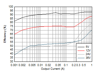
| VOUT = 3.3 V | 1.4 MHz | DDA Package |
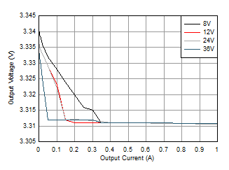
| VOUT = 3.3 V |
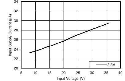
| VOUT = 3.3 V | IOUT = 0 A | RFBT = 1 MΩ |
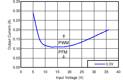
| VOUT = 3.3 V | ƒSW = 400 kHz |
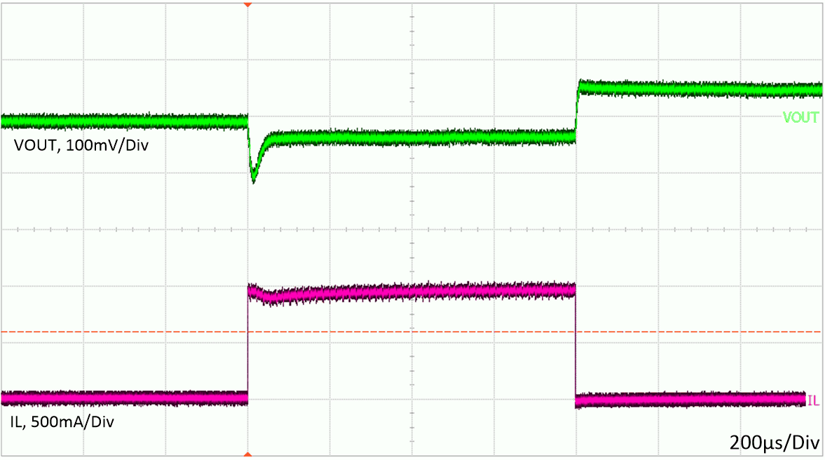
| VIN = 12 V | VOUT = 3.3 V | |
| tf = tr = 2 µs | IOUT = 0 A to 1 A | |
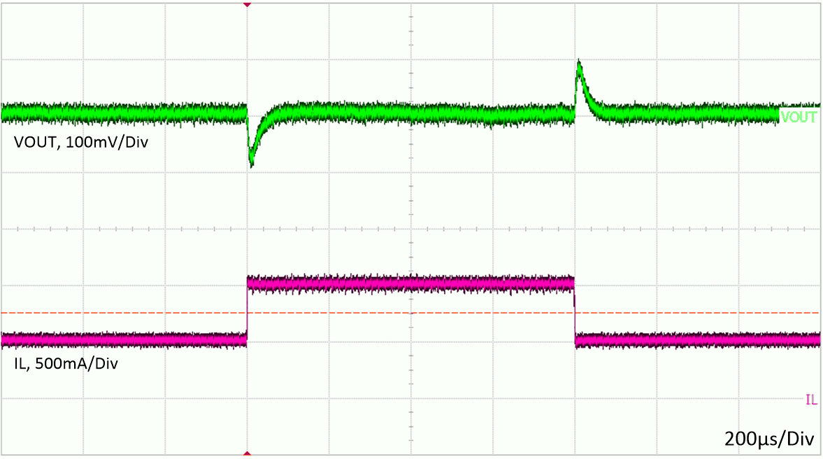
| VIN = 12 V | VOUT = 3.3 V | |
| tf = tr = 2 µs | IOUT = 0.5 A to 1 A | |
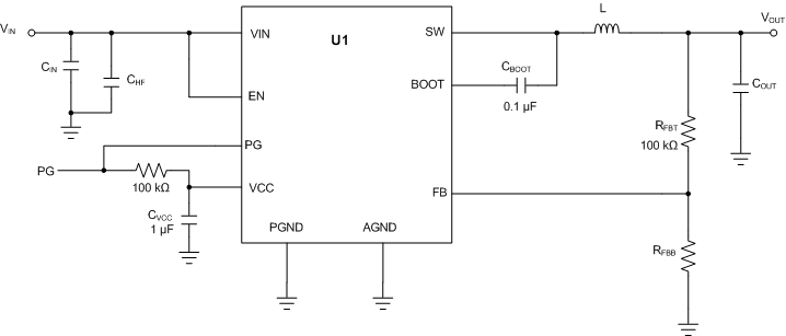 Figure 9-20 Circuit for Application Curves
Table 9-3 BOM for Typical Application Curves DDA
Package
| VOUT(1) | Frequency | RFBB | COUT | CIN + CHF | L | U1 |
|---|---|---|---|---|---|---|
| 3.3 V | 400 kHz | 43.3 kΩ | 4 × 22 µF | 1 × 10 µF + 1 × 220 nF | 6.8 µH, 14 mΩ | LMR33610ADDA |
| 3.3 V | 1400 kHz | 43.3 kΩ | 4 × 22 µF | 1 × 10 µF + 1 × 220 nF | 2.2 µH, 11.4 mΩ | LMR33610BDDA |
| 5 V | 400 kHz | 24.9 kΩ | 4 × 22 µF | 1 × 10 µF + 1 × 220 nF | 8.2 µH, 14 mΩ | LMR33610ADDA |
| 5 V | 1400 kHz | 24.9 kΩ | 4 × 22 µF | 1 × 10 µF + 1 × 220 nF | 2.2 µH, 11.4 mΩ | LMR33610BDDA |
(1) The values in this table were selected to enhance certain performance criteria and may not represent typical values.