ZHCSIE9C June 2018 – October 2020 LMR33620-Q1
PRODUCTION DATA
- 1 特性
- 2 应用
- 3 说明
- 4 修订历史记录
- 5 Pin Configuration and Functions
- 6 Specifications
- 7 Detailed Description
-
8 Application and Implementation
- 8.1 Application Information
- 8.2
Typical Application
- 8.2.1 Design Requirements
- 8.2.2
Detailed Design Procedure
- 8.2.2.1 Custom Design With WEBENCH® Tools
- 8.2.2.2 Choosing the Switching Frequency
- 8.2.2.3 Setting the Output Voltage
- 8.2.2.4 Inductor Selection
- 8.2.2.5 Output Capacitor Selection
- 8.2.2.6 Input Capacitor Selection
- 8.2.2.7 CBOOT
- 8.2.2.8 VCC
- 8.2.2.9 CFF Selection
- 8.2.2.10 External UVLO
- 8.2.2.11 Maximum Ambient Temperature
- 8.2.3 Application Curves
- 8.3 What to Do and What Not to Do
- 9 Power Supply Recommendations
- 10Layout
- 11Device and Documentation Support
封装选项
请参考 PDF 数据表获取器件具体的封装图。
机械数据 (封装 | 引脚)
- RNX|12
散热焊盘机械数据 (封装 | 引脚)
- RNX|12
订购信息
8.2.2.3.1 Fixed Output Voltage Option
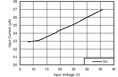
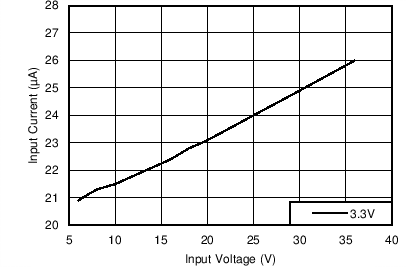
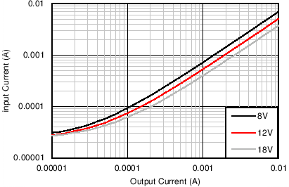
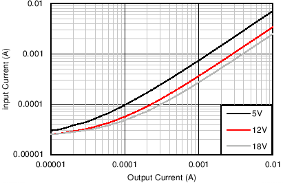
With the fixed output voltage version, the feed-back divider is internal to the device. Therefore, an external divider is not needed and the FB input is connected directly to VOUT. The total resistance of the internal divider is about 2 MΩ (see Section 6.5). The large value of the divider reduces the loading on the output and helps to reduce the no-load input current of the system. For those applications that require the lowest no-load input current, without resorting to large value feed-back resistors, the fixed output voltage option is a good solution. Figure 8-2 and Figure 8-3 show the no-load and light load input supply current for the fixed option, using the BOM from Table 8-3 and with RFBT = 0 Ω and RFBB = open. Figure 8-4 and Figure 8-5 show the same characteristics for the 3.3-V fixed option.
 Figure 8-2 No-load Input Supply Current for 5-V Fixed Output Option
 Figure 8-4 No-load Input Supply Current for 3.3-V Fixed Output Option
 Figure 8-3 Input Supply Current vs Output Current for 5-V Fixed Output Option
 Figure 8-5 Input Supply Current vs Output Current for 3.3-V Fixed Output Option