ZHCSIE9C June 2018 – October 2020 LMR33620-Q1
PRODUCTION DATA
- 1 特性
- 2 应用
- 3 说明
- 4 修订历史记录
- 5 Pin Configuration and Functions
- 6 Specifications
- 7 Detailed Description
-
8 Application and Implementation
- 8.1 Application Information
- 8.2
Typical Application
- 8.2.1 Design Requirements
- 8.2.2
Detailed Design Procedure
- 8.2.2.1 Custom Design With WEBENCH® Tools
- 8.2.2.2 Choosing the Switching Frequency
- 8.2.2.3 Setting the Output Voltage
- 8.2.2.4 Inductor Selection
- 8.2.2.5 Output Capacitor Selection
- 8.2.2.6 Input Capacitor Selection
- 8.2.2.7 CBOOT
- 8.2.2.8 VCC
- 8.2.2.9 CFF Selection
- 8.2.2.10 External UVLO
- 8.2.2.11 Maximum Ambient Temperature
- 8.2.3 Application Curves
- 8.3 What to Do and What Not to Do
- 9 Power Supply Recommendations
- 10Layout
- 11Device and Documentation Support
封装选项
请参考 PDF 数据表获取器件具体的封装图。
机械数据 (封装 | 引脚)
- RNX|12
散热焊盘机械数据 (封装 | 引脚)
- RNX|12
订购信息
7.3.1 Power-Good Flag Output
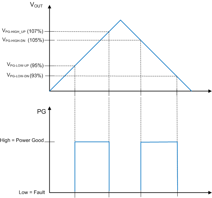
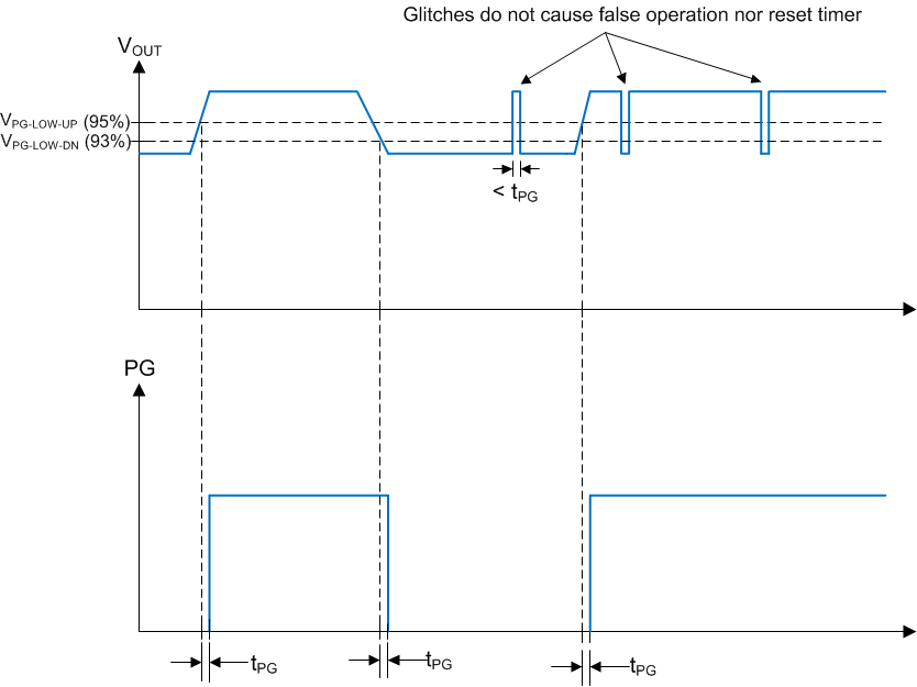
The power-good flag function (PG output pin) of the LMR33620-Q1 can be used to reset a system microprocessor whenever the output voltage is out of regulation. This open-drain output goes low under fault conditions, such as current limit and thermal shutdown, as well as during normal start-up. A glitch filter prevents false flag operation for short excursions of the output voltage, such as during line and load transients. The timing parameters of the glitch filter are found in Section 6.5. Output voltage excursions lasting less than tPG do not trip the power-good flag. Power-good operation can best be understood by reference to Figure 7-1 and Figure 7-2. Note that during initial power up, a delay of about 4 ms (typical) is inserted from the time that EN is asserted to the time that the power-good flag goes high. This delay only occurs during start-up and is not encountered during normal operation of the power-good function.
The power-good output consists of an open-drain NMOS, requiring an external pullup resistor to a suitable logic supply. It can also be pulled up to either VCC or VOUT, through a 100-kΩ resistor, as desired. If this function is not needed, the PG pin must be left floating. When EN is pulled low, the flag output is also forced low. With EN low, power good remains valid as long as the input voltage is ≥ 2 V (typical). Limit the current into the power-good flag pin to less than 5 mA D.C. The maximum current is internally limited to about 35 mA when the device is enabled and about 65 mA when the device is disabled. The internal current limit protects the device from any transient currents that can occur when discharging a filter capacitor connected to this output.
 Figure 7-1 Static Power-Good Operation
 Figure 7-2 Power-Good-Timing Behavior