ZHCSHQ4E February 2018 – November 2020 LMR33620
PRODUCTION DATA
- 1 特性
- 2 应用
- 3 说明
- 4 Revision History
- 5 Device Comparison Table
- 6 Pin Configuration and Functions
- 7 Specifications
- 8 Detailed Description
-
9 Application and Implementation
- 9.1 Application Information
- 9.2
Typical Application
- 9.2.1 Design Requirements
- 9.2.2
Detailed Design Procedure
- 9.2.2.1 Custom Design With WEBENCH® Tools
- 9.2.2.2 Choosing the Switching Frequency
- 9.2.2.3 Setting the Output Voltage
- 9.2.2.4 Inductor Selection
- 9.2.2.5 Output Capacitor Selection
- 9.2.2.6 Input Capacitor Selection
- 9.2.2.7 CBOOT
- 9.2.2.8 VCC
- 9.2.2.9 CFF Selection
- 9.2.2.10 External UVLO
- 9.2.2.11 Maximum Ambient Temperature
- 9.2.3 Application Curves
- 9.3 What to Do and What Not to Do
- 10Layout
- 11Device and Documentation Support
封装选项
请参考 PDF 数据表获取器件具体的封装图。
机械数据 (封装 | 引脚)
- RNX|12
- DDA|8
散热焊盘机械数据 (封装 | 引脚)
订购信息
8.4.3 Minimum Switch On-Time
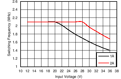
Every switching regulator has a minimum controllable on-time dictated by the inherent delays and blanking times associated with the control circuits. This imposes a minimum switch duty cycle and, therefore, a minimum conversion ratio. The constraint is encountered at high input voltages and low output voltages. To help extend the minimum controllable duty cycle, the LMR33620 automatically reduces the switching frequency when the minimum on-time limit is reached. This way the converter can regulate the lowest programmable output voltage at the maximum input voltage. An estimate for the approximate input voltage, for a given output voltage, before frequency foldback occurs is found in Equation 2. The values of tON and fSW can be found in Section 7.5. As the input voltage is increased, the switch on-time (duty-cycle) reduces to regulate the output voltage. When the on-time reaches the limit, the switching frequency drops, while the on-time remains fixed. This relationship is highlighted in Figure 8-13 for a nominal switching frequency of 2.1 MHz.

 Figure 8-13 Switching Frequency versus Input Voltage VOUT = 3.3 V