ZHCSIE8C June 2018 – October 2020 LMR33630-Q1
PRODUCTION DATA
- 1 特性
- 2 应用
- 3 说明
- 4 Revision History
- 5 Pin Configuration and Functions
- 6 Specifications
- 7 Detailed Description
-
8 Application and Implementation
- 8.1 Application Information
- 8.2
Typical Application
- 8.2.1 Design Requirements
- 8.2.2
Detailed Design Procedure
- 8.2.2.1 Custom Design With WEBENCH® Tools
- 8.2.2.2 Choosing the Switching Frequency
- 8.2.2.3 Setting the Output Voltage
- 8.2.2.4 Inductor Selection
- 8.2.2.5 Output Capacitor Selection
- 8.2.2.6 Input Capacitor Selection
- 8.2.2.7 CBOOT
- 8.2.2.8 VCC
- 8.2.2.9 CFF Selection
- 8.2.2.10 External UVLO
- 8.2.2.11 Maximum Ambient Temperature
- 8.2.3 Application Curves
- 8.3 What to Do and What Not to Do
- 9 Power Supply Recommendations
- 10Layout
- 11Device and Documentation Support
封装选项
请参考 PDF 数据表获取器件具体的封装图。
机械数据 (封装 | 引脚)
- RNX|12
散热焊盘机械数据 (封装 | 引脚)
- RNX|12
订购信息
7.4.2 Dropout
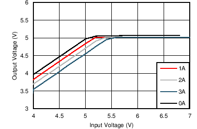
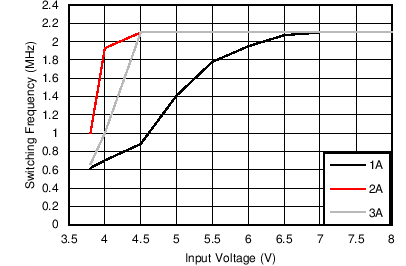
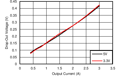
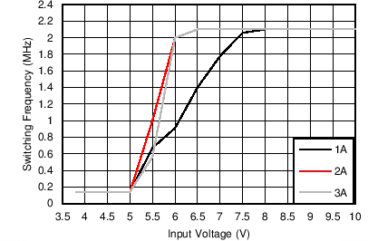
The dropout performance of any buck regulator is affected by the RDSON of the power MOSFETs, the DC resistance of the inductor, and the maximum duty cycle that the controller can achieve. As the input voltage level approaches the output voltage, the off-time of the high-side MOSFET starts to approach the minimum value (see Section 6.6). Beyond this point, the switching can become erratic, and the output voltage falls out of regulation. To avoid this problem, the LMR33630-Q1 automatically reduces the switching frequency to increase the effective duty cycle and maintain regulation. In this data sheet, the dropout voltage is defined as the difference between the input and output voltage when the output has dropped by 1% of its nominal value. Under this condition, the switching frequency has dropped to its minimum value of about 140 kHz. Note that the 0.4 V short circuit detection threshold is not activated when in dropout mode. Typical dropout characteristics can be found in Figure 7-9, Figure 7-10, Figure 7-11, and Figure 7-12.
 Figure 7-9 Overall Dropout Characteristic VOUT = 5 V
 Figure 7-11 Typical Switching Frequency in Dropout Mode
VOUT = 3.3 V, fSW = 2.1
MHz
 Figure 7-10 Typical Dropout Voltage versus Output Current in Frequency Foldback ƒSW = 140 kHz
 Figure 7-12 Typical Switching Frequency in Dropout Mode
VOUT = 5 V, fSW = 2.1
MHz