ZHCSJO4A May 2019 – October 2019 LMR34206-Q1
PRODUCTION DATA.
- 1 特性
- 2 应用
- 3 说明
- 4 修订历史记录
- 5 Device Comparison Table
- 6 Pin Configuration and Functions
- 7 Specifications
- 8 Detailed Description
- 9 Application and Implementation
- 10Power Supply Recommendations
- 11Layout
- 12器件和文档支持
- 13机械、封装和可订购信息
8.3.1 Power-Good Flag Output
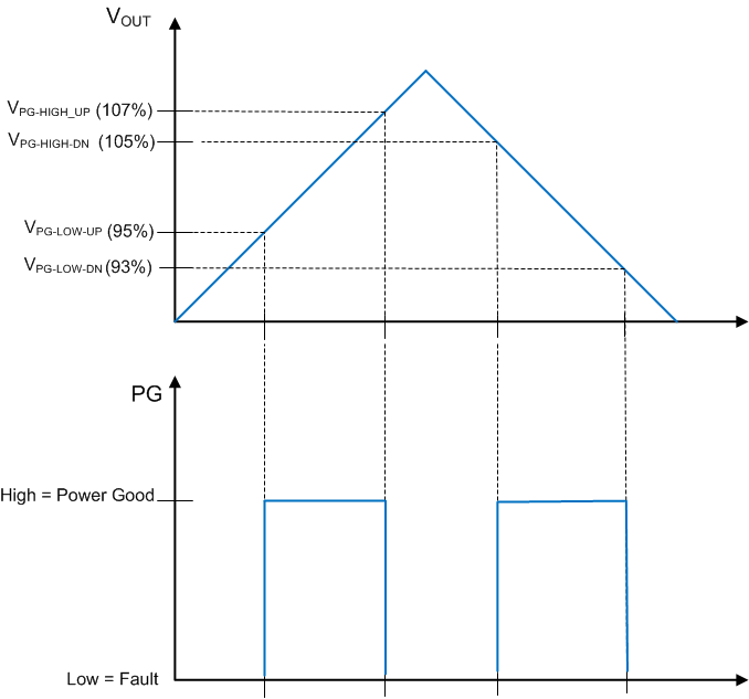
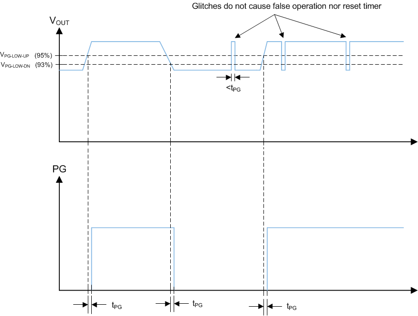
The power-good flag function (PG output pin) of the LMR34206-Q1 can be used to reset a system microprocessor whenever the output voltage is out of regulation. This open-drain output goes low under fault conditions, such as current limit and thermal shutdown, as well as during normal start-up. A glitch filter prevents false flag operation for short excursions of the output voltage, such as during line and load transients. Output voltage excursions lasting less than tPG do not trip the power-good flag. Power-good operation can best be understood by reference to Figure 8 and Figure 9. Note that during initial power-up a delay of about 4 ms (typical) is inserted from the time that EN is asserted to the time that the power-good flag goes high. This delay only occurs during start-up and is not encountered during normal operation of the power-good function.
The power-good output consists of an open drain NMOS; requiring an external pullup resistor to a suitable logic supply. It can also be pulled up to either VCC or VOUT, through an appropriate resistor, as desired. If this function is not needed, the PG pin must be grounded. When EN is pulled low, the flag output is also forced low. With EN low, power good remains valid as long as the input voltage is ≥ 2 V (typical). Limit the current into this pin to ≤ 4 mA.
 Figure 8. Static Power-Good Operation
  Figure 9. Power-Good-Timing Behavior