ZHCSJO4A May 2019 – October 2019 LMR34206-Q1
PRODUCTION DATA.
- 1 特性
- 2 应用
- 3 说明
- 4 修订历史记录
- 5 Device Comparison Table
- 6 Pin Configuration and Functions
- 7 Specifications
- 8 Detailed Description
- 9 Application and Implementation
- 10Power Supply Recommendations
- 11Layout
- 12器件和文档支持
- 13机械、封装和可订购信息
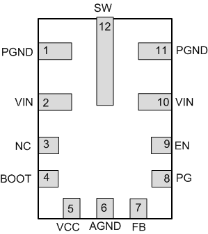
6 Pin Configuration and Functions
RNX Package
12-Pin VQFN-HR
Top View

Pin Functions
| NO. | NAME | TYPE | DESCRIPTION |
|---|---|---|---|
| 1, 11 | PGND | G | Power ground terminal. Connect to system ground and AGND. Connect to CIN with short wide traces. |
| 2, 10 | VIN | P | Input supply to regulator. Connect to CIN with short wide traces. |
| 3 | NC | — | Connect the SW pin to NC on the PCB. This simplifies the connection from the CBOOT capacitor to the SW pin. This pin has no internal connection to the regulator. |
| 4 | BOOT | P | Boot-strap supply voltage for internal high-side driver. Connect a high-quality 100-nF capacitor from this pin to the SW pin. Connect the SW pin to NC on the PCB. This simplifies the connection from the CBOOT capacitor to the SW pin. |
| 5 | VCC | P | Internal 5-V LDO output. Used as supply to internal control circuits. Do not connect to external loads. Can be used as logic supply for power-good flag. Connect a high-quality 1-µF capacitor from this pin to GND. |
| 6 | AGND | G | Analog ground for regulator and system. Ground reference for internal references and logic. All electrical parameters are measured with respect to this pin. Connect to system ground on PCB. |
| 7 | FB | A | Feedback input to regulator. Connect to tap point of feedback voltage divider. DO NOT FLOAT. DO NOT GROUND. |
| 8 | PG | A | Open drain power-good flag output. Connect to suitable voltage supply through a current limiting resistor. High = power OK, low = power bad. Goes low when EN = Low. Can be open or grounded when not used. |
| 9 | EN | A | Enable input to regulator. High = ON, low = OFF. Can be connected directly to VIN; DO NOT FLOAT. |
| 12 | SW | P | Regulator switch node. Connect to power inductor. Connect the SW pin to NC on the PCB. This simplifies the connection from the CBOOT capacitor to the SW pin. |
| A = Analog, P = Power, G = Ground | |||