ZHCSJO3B May   2019  – November 2020 LMR34215-Q1

PRODUCTION DATA  

  1. 特性
  2. 应用
  3. 说明
  4. Revision History
  5. Device Comparison Table
  6. Pin Configuration and Functions
  7. Specifications
    1. 7.1 Absolute Maximum Ratings
    2. 7.2 ESD Ratings
    3. 7.3 Recommended Operating Conditions
    4. 7.4 Thermal Information
    5. 7.5 Electrical Characteristics
    6. 7.6 Timing Requirements
    7. 7.7 System Characteristics
    8. 7.8 Typical Characteristics
  8. Detailed Description
    1. 8.1 Overview
    2. 8.2 Functional Block Diagram
    3. 8.3 Feature Description
      1. 8.3.1 Power-Good Flag Output
      2. 8.3.2 Enable and Start-up
      3. 8.3.3 Current Limit and Short Circuit
      4. 8.3.4 Undervoltage Lockout and Thermal Shutdown
    4. 8.4 Device Functional Modes
      1. 8.4.1 Auto Mode
      2. 8.4.2 Forced PWM Operation
      3. 8.4.3 Dropout
      4. 8.4.4 Minimum Switch On-Time
      5. 8.4.5 Spread Spectrum Operation
  9. Power Supply Recommendations
  10. 10Layout
    1. 10.1 Layout Guidelines
      1. 10.1.1 Ground and Thermal Considerations
    2. 10.2 Layout Example
  11. 11Device and Documentation Support
    1. 11.1 Device Support
      1. 11.1.1 Development Support
    2. 11.2 Documentation Support
      1. 11.2.1 Related Documentation
    3. 11.3 Receiving Notification of Documentation Updates
    4. 11.4 Support Resources
    5. 11.5 Trademarks
    6. 11.6 Electrostatic Discharge Caution
    7. 11.7 Glossary
  12. 12Mechanical, Packaging, and Orderable Information

封装选项

机械数据 (封装 | 引脚)
散热焊盘机械数据 (封装 | 引脚)
订购信息

Application Curves

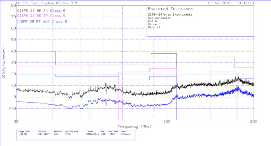
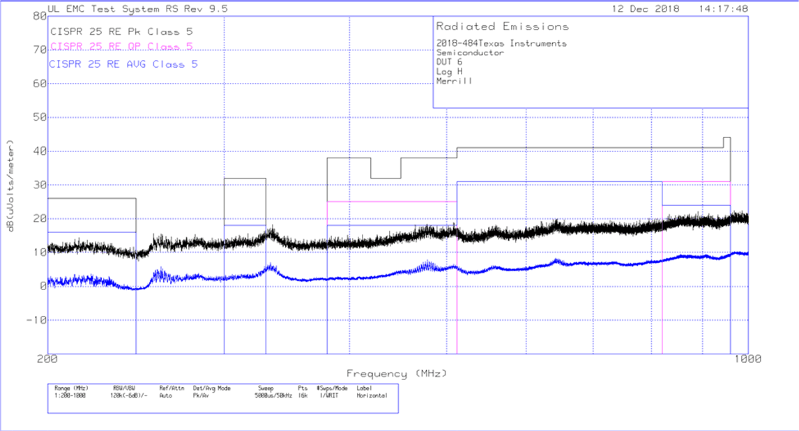
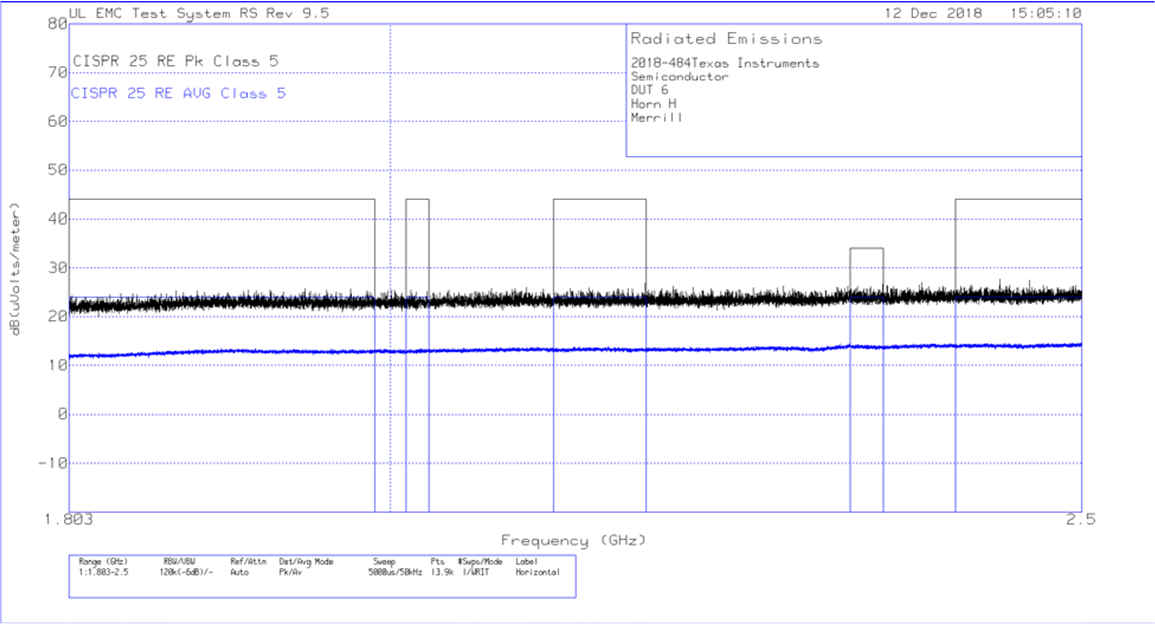
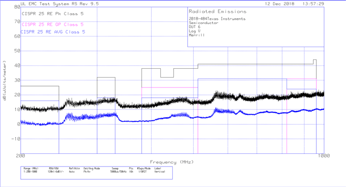
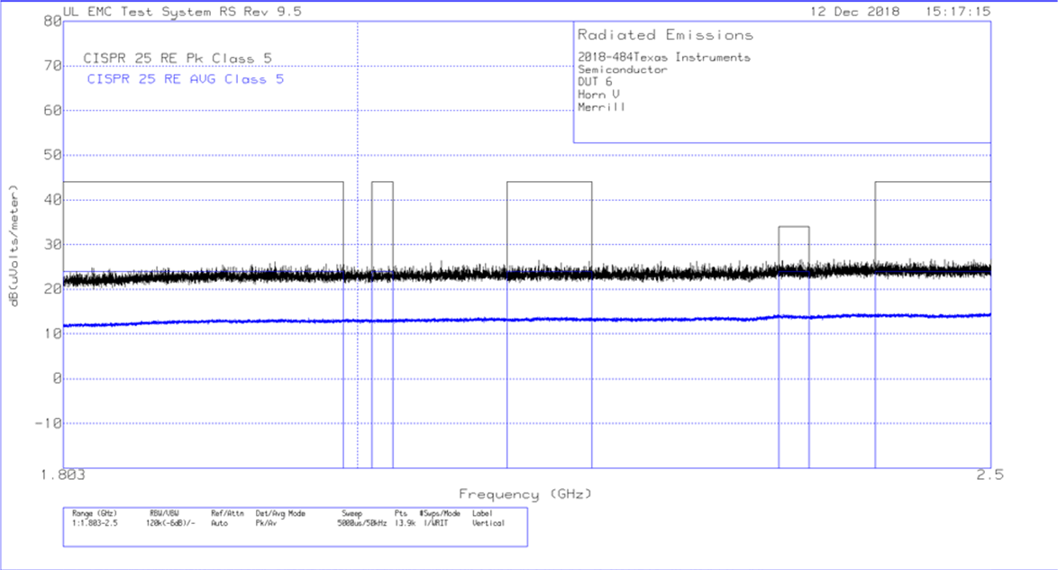
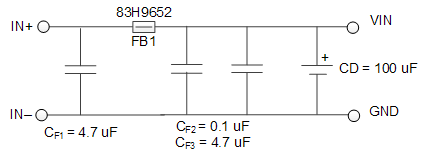
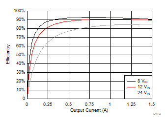
Unless otherwise specified the following conditions apply: VIN = 12 V, TA = 25°C. The circuit is shown in Figure 9-2, with the BOM from Table 9-3. Figure 9-5 through Figure 9-20 show the conducted and radiated emissions performance tested against the CISPR25 Class 5 limits. For the conducted EMI results the limit lines labeled "AV5" represent the average limits, and the limit lines labeled "PK5" represent the peak limits. For the radiated EMI results, the blue limit lines represent the average limits, and the black limit lines represent the peak limits.
GUID-2B2936F0-9DCD-4613-BC50-027363770B02-low.gif
VOUT = 5 V 2100 kHz
Figure 9-5 Efficiency
GUID-CF21BCDD-25C9-401A-B2D2-05E2C7C19AD5-low.gif
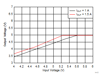
VOUT = 5 V 2100 kHz
Figure 9-7 Overall Dropout Curve
GUID-2593C441-23CF-4CC6-8A2B-D264335BC742-low.jpg
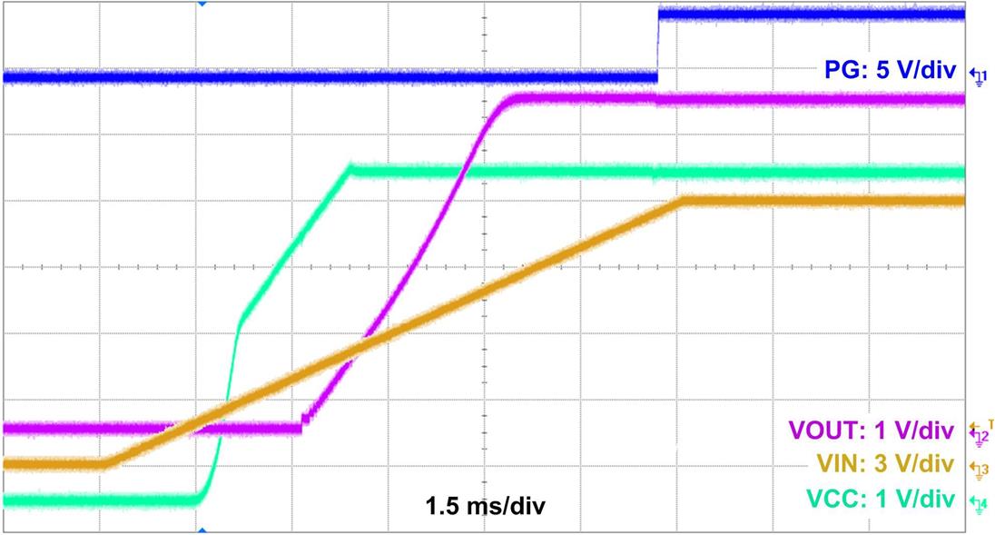
VOUT = 5 V 2100 kHz
Figure 9-9 Start-Up Waveform
GUID-BD5F896F-4000-4F67-92D0-D8E03932B8B1-low.gif
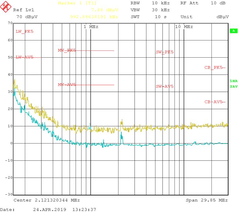
VIN = 13.5 V VOUT = 5 V IOUT = 1.5 A
Frequency Tested: 150kHz to 30 MHz
Figure 9-11 Conducted EMI vs. CISPR25 Limits (Yellow: Peak Signal, Blue: Average Signal)
GUID-D281354C-75EE-4ACA-89ED-5C44F77ACCA9-low.gif
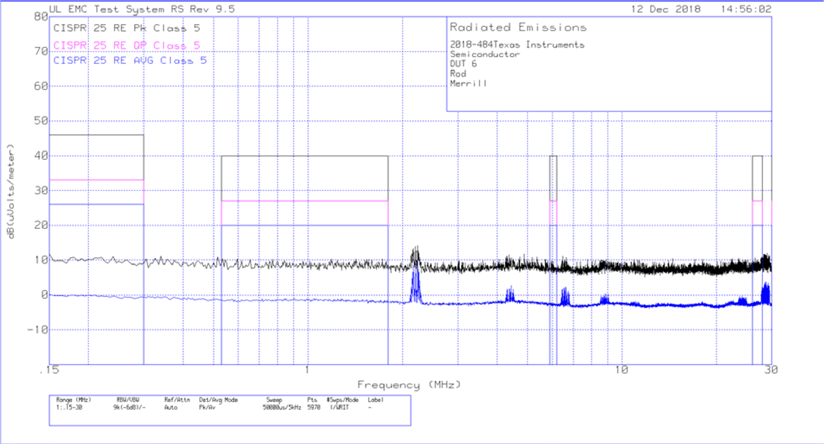
VIN = 13.5 V VOUT = 5 V IOUT = 1.5 A
Frequency Tested: 150 kHz to 30 MHz
Figure 9-13 Radiated EMI Rod vs. CISPR25 Limits
GUID-2670F2C6-1A86-4804-84EB-15CA1C2663B9-low.gif
VIN = 13.5 V VOUT = 5 V IOUT = 1.5 A
Frequency Tested: 30 MHz to 200 MHz
Figure 9-15 Radiated EMI Bicon Horizontal vs. CISPR25 Limits
GUID-8418793B-ED8E-4212-99AB-788F264F9D73-low.gif
VIN = 13.5 V VOUT = 5 V IOUT = 1.5 A
Frequency Tested: 200 MHz to 1 GHz
Figure 9-17 Radiated EMI Log Horizontal vs. CISPR25 Limits
GUID-FDABBD51-BBAF-4AF2-9C00-162B3B7A2D3A-low.gif
VIN = 13.5 V VOUT = 5 V IOUT = 1.5 A
Frequency Tested: 1.8 GHz to 2.5 GHz
Figure 9-19 Radiated EMI Horn Horizontal vs. CISPR25 Limits
GUID-0637CACD-4504-4B84-BA7C-FD65E1E5B1A6-low.gif
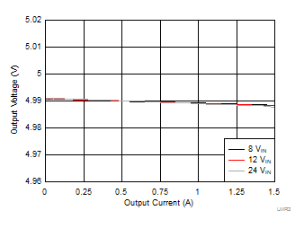
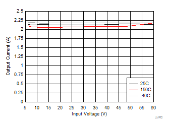
VOUT = 5 V 2100 kHz
Figure 9-6 Load Regulation
GUID-1D0AEF26-FA39-4549-BD39-D1DDAA9A3FD2-low.gif
VOUT = 5 V 2100 kHz
Figure 9-8 Load Current to Trigger Short Circuit
GUID-6CD360D7-0837-47B2-8413-64D6823F2DA6-low.jpg
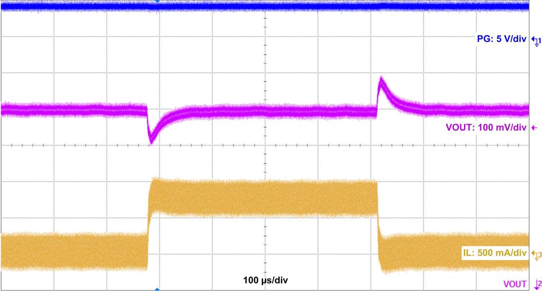
VOUT = 5 V Slew Rate = 1 A/µs 2100 kHz ILOAD= 0 A - 0.75 A
Figure 9-10 Load Transient Waveform
GUID-E2B3B7CC-3F2B-4929-BEFB-B59FC878ACDA-low.gif
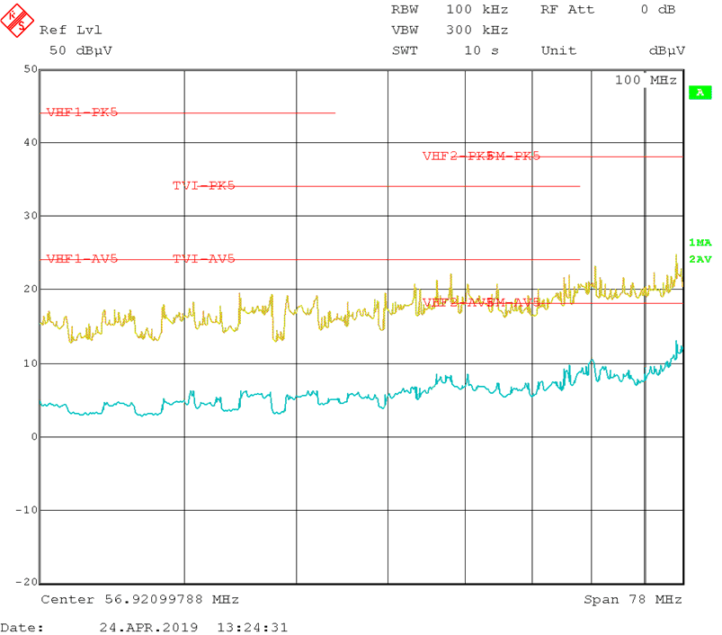
VIN = 13.5 V VOUT = 5 V IOUT = 1.5 A
Frequency Tested: 30 MHz to 108 MHz
Figure 9-12 Conducted EMI vs. CISPR25 Limits (Yellow: Peak Signal, Blue: Average Signal)
GUID-E07D1D9A-C3E3-4786-850A-F45087EF1730-low.gif
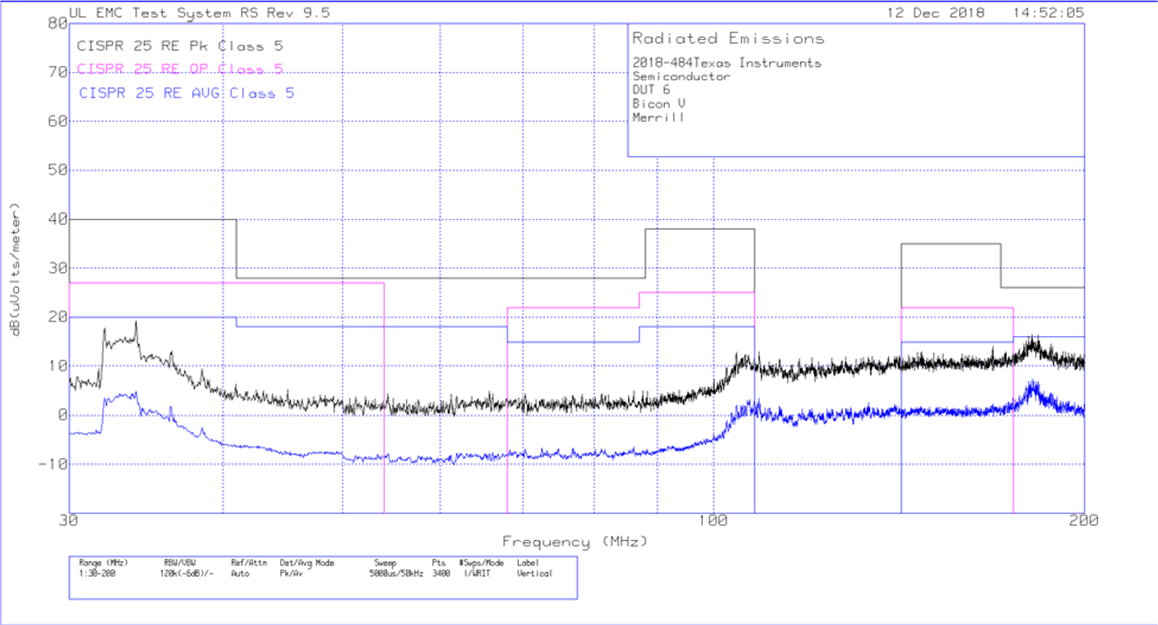
VIN = 13.5 V VOUT = 5 V IOUT = 1.5 A
Frequency Tested: 30 MHz to 200 MHz
Figure 9-14 Radiated EMI Bicon Vertical vs. CISPR25 Limits
GUID-8379BC52-2940-4599-B67A-C886F196674E-low.gif
VIN = 13.5 V VOUT = 5 V IOUT = 1.5 A
Frequency Tested: 200 MHz to 1 GHz
Figure 9-16 Radiated EMI Log Vertical vs. CISPR25 Limits
GUID-983B9512-2159-4271-9687-0081095A113D-low.gif
VIN = 13.5 V VOUT = 5 V IOUT = 1.5 A
Frequency Tested: 1.83 GHz to 2.5 GHz
Figure 9-18 Radiated EMI Horn Vertical vs. CISPR25 Limits
GUID-B826DA35-38CB-408D-AE77-F055BE732404-low.gif


Figure 9-20 Recommended Input EMI Filter