ZHCSJO3B May 2019 – November 2020 LMR34215-Q1
PRODUCTION DATA
- 1 特性
- 2 应用
- 3 说明
- 4 Revision History
- 5 Device Comparison Table
- 6 Pin Configuration and Functions
- 7 Specifications
- 8 Detailed Description
- 9 Power Supply Recommendations
- 10Layout
- 11Device and Documentation Support
- 12Mechanical, Packaging, and Orderable Information
8.4.4 Minimum Switch On-Time
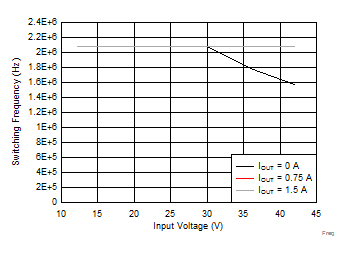
Every switching regulator has a minimum controllable on-time dictated by the inherent delays and blanking times associated with the control circuits. This imposes a minimum switch duty cycle and, therefore, a minimum conversion ratio. The constraint is encountered at high input voltages and low output voltages. To help extend the minimum controllable duty cycle, the LMR34215-Q1 automatically reduces the switching frequency when the minimum on-time limit is reached. This way, the converter can regulate the lowest programmable output voltage at the maximum input voltage. An estimate for the approximate input voltage, for a given output voltage, before frequency foldback occurs, is found in Equation 2. As the input voltage is increased, the switch on-time (duty cycle) reduces to regulate the output voltage. When the on-time reaches the limit, the switching frequency drops, while the on-time remains fixed.

 Figure 8-11 Switching Frequency vs Input Voltage VOUT = 5 V