ZHCSKX8B September   2019  – September 2020 LMR36503-Q1

PRODUCTION DATA  

  1. 特性
  2. 应用
  3. 说明
  4. Revision History
  5. Device Comparison Table
  6. Pin Configuration and Functions
    1.     Pin Functions
  7. Specifications
    1. 7.1 Absolute Maximum Ratings
    2. 7.2 ESD (Automotive) Ratings
    3. 7.3 Recommended Operating Conditions
    4. 7.4 Thermal Information
    5. 7.5 Electrical Characteristics
    6. 7.6 Timing Characteristics
    7. 7.7 Switching Characteristics
    8. 7.8 System Characteristics
    9. 7.9 Typical Characteristics
  8. Detailed Description
    1. 8.1 Overview
    2. 8.2 Functional Block Diagram
    3. 8.3 Feature Description
      1. 8.3.1  Enable, Start-up and Shutdown
      2. 8.3.2  External CLK SYNC (with MODE/SYNC)
        1. 8.3.2.1 Pulse-Dependent MODE/SYNC Pin Control
      3. 8.3.3  Adjustable Switching Frequency (with RT)
      4. 8.3.4  Power-Good Output Operation
      5. 8.3.5  Internal LDO, VCC UVLO, and VOUT/BIAS Input
      6. 8.3.6  Bootstrap Voltage and VCBOOT-UVLO (CBOOT Terminal)
      7. 8.3.7  Output Voltage Selection
      8. 8.3.8  Soft Start and Recovery from Dropout
        1. 8.3.8.1 Recovery from Dropout
      9. 8.3.9  Current Limit and Short Circuit
      10. 8.3.10 Thermal Shutdown
      11. 8.3.11 Input Supply Current
    4. 8.4 Device Functional Modes
      1. 8.4.1 Shutdown Mode
      2. 8.4.2 Standby Mode
      3. 8.4.3 Active Mode
        1. 8.4.3.1 CCM Mode
        2. 8.4.3.2 Auto Mode - Light Load Operation
          1. 8.4.3.2.1 Diode Emulation
          2. 8.4.3.2.2 Frequency Reduction
        3. 8.4.3.3 FPWM Mode - Light Load Operation
        4. 8.4.3.4 Minimum On-time (High Input Voltage) Operation
        5. 8.4.3.5 Dropout
  9. Application and Implementation
    1. 9.1 Application Information
    2. 9.2 Typical Application
      1. 9.2.1 Design Requirements
      2. 9.2.2 Detailed Design Procedure
        1. 9.2.2.1 Choosing the Switching Frequency
        2. 9.2.2.2 Setting the Output Voltage
          1. 9.2.2.2.1 FB for Adjustable Output
        3. 9.2.2.3 Inductor Selection
        4. 9.2.2.4 Output Capacitor Selection
        5. 9.2.2.5 Input Capacitor Selection
        6. 9.2.2.6 CBOOT
        7. 9.2.2.7 VCC
        8. 9.2.2.8 CFF Selection
          1. 9.2.2.8.1 External UVLO
        9. 9.2.2.9 Maximum Ambient Temperature
      3. 9.2.3 Application Curves
    3. 9.3 What to Do and What Not to Do
  10. 10Power Supply Recommendations
  11. 11Layout
    1. 11.1 Layout Guidelines
      1. 11.1.1 Ground and Thermal Considerations
    2. 11.2 Layout Example
  12. 12Device and Documentation Support
    1. 12.1 Documentation Support
      1. 12.1.1 Related Documentation
    2. 12.2 接收文档更新通知
    3. 12.3 支持资源
    4. 12.4 Trademarks
    5. 12.5 静电放电警告
    6. 12.6 术语表
  13. 13Mechanical, Packaging, and Orderable Information

封装选项

机械数据 (封装 | 引脚)
散热焊盘机械数据 (封装 | 引脚)
订购信息

Application Curves

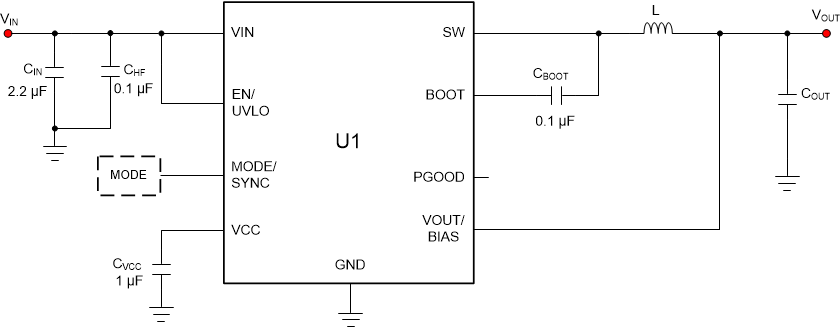
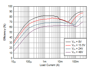
Unless otherwise specified the following conditions apply: VIN = 13.5V, TA = 25°C. Figure 9-25 shows the circuit with the appropriate BOM in Table 9-3
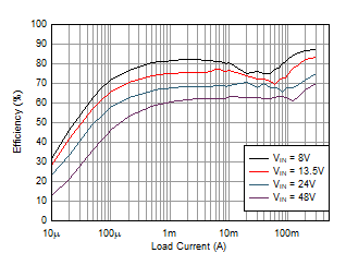
Unless otherwise specified the following conditions apply: VIN = 13.5V, TA = 25°C. Figure 9-25 shows the circuit with the appropriate BOM in Table 9-3 GUID-20200811-CA0I-NCLF-2TP0-GHGT7HP47JSX-low.gif
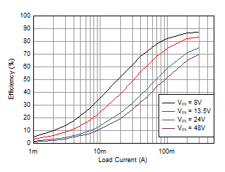
LMR36503MSC3 VOUT = 3.3 V Fixed 2.2 MHz (AUTO)
Figure 9-4 Efficiency. Unless otherwise specified the following conditions apply: VIN = 13.5V, TA = 25°C. Figure 9-25 shows the circuit with the appropriate BOM in Table 9-3
GUID-20200813-CA0I-22HG-ZPFR-2STGCFWFNTKR-low.gif
LMR36503MSC5 VOUT = 5 V Fixed 2.2 MHz (AUTO)
Figure 9-6 Efficiency
GUID-20200813-CA0I-DG4Q-2PLH-FTMRQ6LT01SJ-low.gif
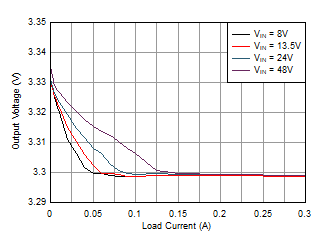
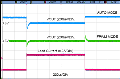
LMR36503MSC3 VOUT = 3.3 V Fixed 2.2 MHz (AUTO)
Figure 9-8 Line and Load Regulation
GUID-20200814-CA0I-Q2B6-PCP9-Z5R22NKS0X0V-low.gif
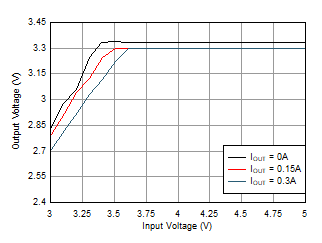
LMR36503MSC3 VOUT = 3.3 V Fixed 2.2 MHz (AUTO)
Figure 9-10 Dropout
GUID-20200817-CA0I-KVH8-SMNF-FRWC9BPMMQSB-low.gif
LMR36503MSC3 VOUT = 3.3 V Fixed 2.2 MHz
0 A to 0.3 A,1 A/µs
Figure 9-12 Load Transient
GUID-20200817-CA0I-CGS5-T3TG-QWGSR2SWGQLZ-low.gif
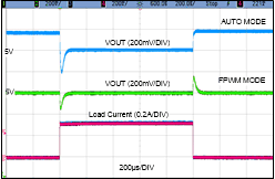
LMR36503MSC5 VOUT = 5 V Fixed 2.2 MHz
0 A to 0.3 A,1 A/µs
Figure 9-14 Load Transient
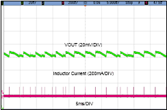
GUID-20200817-CA0I-RXZ0-LG3N-XJLLRWFMHN70-low.gif
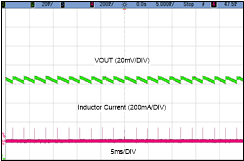
LMR36503MSC3 VOUT = 3.3 V Fixed No Load
Figure 9-16 Output Ripple
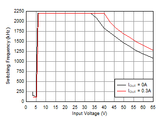
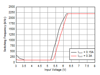
GUID-20200906-CA0I-F1H0-6SBB-CVRPLMDZTHNJ-low.gif
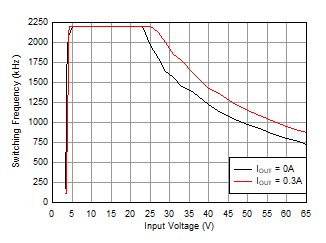
LMR36503MSC3 VOUT = 3.3 V Fixed 2200 kHz
FPWM
Figure 9-18 Switching Frequency over Input Voltage
GUID-20200906-CA0I-FPT4-4DF8-WQ42CPH4GMKS-low.gif
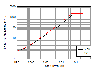
LMR36503MSC3 VOUT = 3.3 V Fixed VIN = 13.5 V
LMR36503MSC5 VOUT = 5 V Fixed AUTO
Figure 9-20 Switching Frequency over Load Current
GUID-20200920-CA0I-ZFLG-1XQJ-8PBMNZS2NK1W-low.png
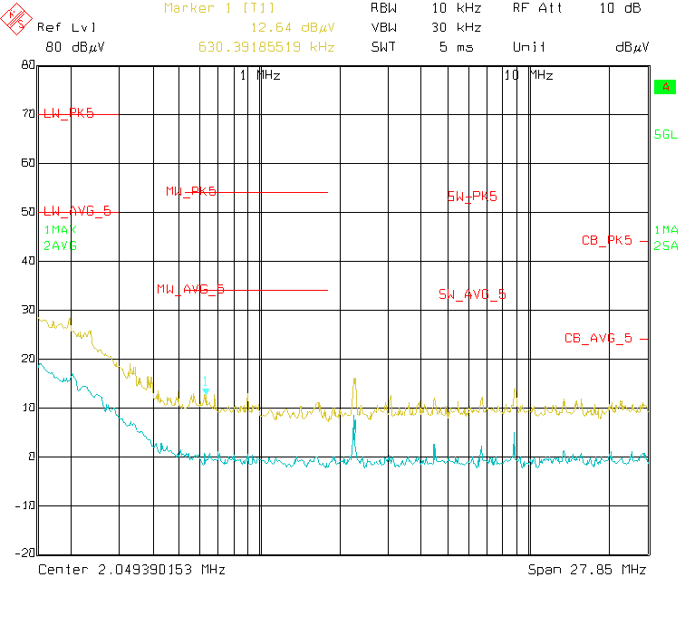
VIN = 13.5 V VOUT = 5 V Fsw = 2.2 MHz
Load = 0.3 A
Figure 9-22 Typical CISPR 25 Conducted EMI 150kHz - 30MHz Yellow: Peak Detect, Blue = Average Detect
GUID-20200813-CA0I-VSFR-JSNG-3B41NZG64MSB-low.gif
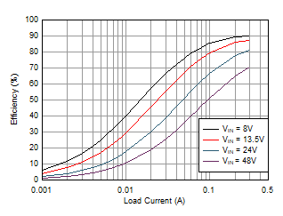
LMR36503MSC3 VOUT = 3.3 V Fixed 2.2 MHz (FPWM)
Figure 9-5 Efficiency
GUID-20200813-CA0I-4D0N-DXHD-CG1VGH0F007B-low.gif
LMR36503MSC5 VOUT = 5 V Fixed 2.2 MHz (FPWM)
Figure 9-7 Efficiency
GUID-20200813-CA0I-M9LP-CNPT-T2JKKCMHXV98-low.gif
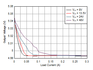
LMR36503MSC5 VOUT = 5 V Fixed 2.2 MHz (AUTO)
Figure 9-9 Line and Load Regulation
GUID-20200814-CA0I-LJVQ-WBQD-ML3PRBR56WJ0-low.gif
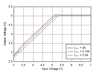
LMR36503MSC5 VOUT = 5 V Fixed 2.2 MHz (AUTO)
Figure 9-11 Dropout
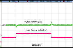
GUID-20200817-CA0I-MHNQ-WXKD-DVV5DZVTRSPV-low.gif
LMR36503MSC3 VOUT = 3.3 V Fixed 2.2 MHz
0.15 A to 0.3 A,1 A/µs
Figure 9-13 Load Transient
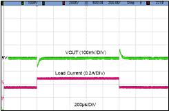
GUID-20200817-CA0I-6ZKK-XRSP-PTXQPML6JF7X-low.gif
LMR36503MSC5 VOUT = 5 V Fixed 2.2 MHz
0.15 A to 0.3 A,1 A/µs
Figure 9-15 Load Transient
GUID-20200817-CA0I-94BM-JLKH-TTCQTKN8RSHB-low.gif
LMR36503MSC5 VOUT = 5 V Fixed No Load
Figure 9-17 Output Ripple
GUID-20200906-CA0I-V6RR-GZX9-TZVPGRNJJ0FW-low.gif
LMR36503MSC5 VOUT = 5 V Fixed 2200 kHz
FPWM
Figure 9-19 Switching Frequency over Input Voltage
GUID-20200906-CA0I-LG4S-4QCL-KKKRTMXMMCKX-low.gif
LMR36503MSC5 VOUT = 5 V Fixed AUTO
Figure 9-21 Switching Frequency during Dropout
GUID-20200920-CA0I-SZTR-2K6R-SH0VS2QH6D2D-low.png
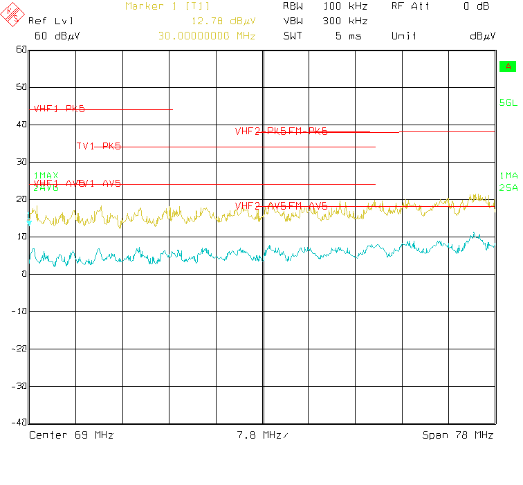
VIN = 13.5 V VOUT = 5 V Fsw = 2.2 MHz
Load = 0.3 A
Figure 9-23 Typical CISPR 25 Conducted EMI 30MHz - 108MHz Yellow: Peak Detect, Blue = Average Detect
GUID-3F1F4F96-03B8-4ECE-87B9-0AD04EA14908-low.gif
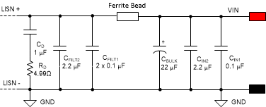
Ferrite Bead Part Number: FBMH3225HM601NT
Figure 9-24 Typical Input EMI Filter for 2.2 MHz
GUID-9A2324FA-0875-459F-96A4-E9C0528E1B81-low.gif Figure 9-25 Schematic for Typical Application Curves
Table 9-3 BOM for Typical Application Curves
U1ƒSWVOUTLNOMINAL COUT
(RATED CAPACITANCE)
LMR36503MSC3RPERQ12200 kHz3.3 V15 µH. 260 mΩ1 × 10 µF
LMR36503MSC5RPERQ12200 kHz5 V15 µH. 260 mΩ1 × 10 µF