ZHCSKB5A October 2019 – February 2020 LMR36510
PRODUCTION DATA.
- 1 特性
- 2 应用
- 3 说明
- 4 修订历史记录
- 5 Pin Configuration and Functions
- 6 Specifications
- 7 Detailed Description
- 8 Application and Implementation
- 9 Power Supply Recommendations
- 10Layout
- 11器件和文档支持
- 12机械、封装和可订购信息
7.4.1 Auto Mode
In auto mode, the device moves between PWM and PFM as the load changes. At light loads, the regulator operates in PFM. At higher loads, the mode changes to PWM.
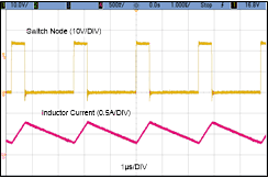
In PWM, the regulator operates as a constant frequency, current mode, full-synchronous converter using PWM to regulate the output voltage. While operating in this mode, the output voltage is regulated by switching at a constant frequency and modulating the duty cycle to control the power to the load. This provides excellent line and load regulation and low output voltage ripple.
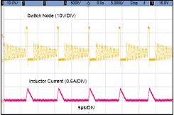
In PFM, the high-side MOSFET is turned on in a burst of one or more pulses to provide energy to the load. The duration of the burst depends on how long it takes the inductor current to reach IPEAK-MIN. The frequency of these bursts is adjusted to regulate the output, while diode emulation is used to maximize efficiency (see the Glossary). This mode provides high light-load efficiency by reducing the amount of input supply current required to regulate the output voltage at small loads. This trades off very good light-load efficiency for larger output voltage ripple and variable switching frequency. Also, a small increase in output voltage occurs at light loads. The actual switching frequency and output voltage ripple depend on the input voltage, output voltage, and load.
 Figure 9. Typical PFM Switching Waveforms
VIN = 24 V, VOUT = 5 V, IOUT = 50 mA
 Figure 10. Typical PWM Switching Waveforms
VIN = 24 V, VOUT = 5 V, IOUT = 0.5 A, ƒS = 400 kHz