ZHCSKB5A October   2019  – February 2020 LMR36510

PRODUCTION DATA.  

  1. 特性
  2. 应用
  3. 说明
    1.     Device Images
      1.      效率与输出电流间的关系 VOUT = 5V,400kHz
      2.      简化原理图
  4. 修订历史记录
  5. Pin Configuration and Functions
    1.     Pin Functions
  6. Specifications
    1. 6.1 Absolute Maximum Ratings
    2. 6.2 ESD Ratings
    3. 6.3 Recommended Operating Conditions
    4. 6.4 Thermal Information
    5. 6.5 Electrical Characteristics
    6. 6.6 Timing Requirements
    7. 6.7 Switching Characteristics
    8. 6.8 System Characteristics
    9. 6.9 Typical Characteristics
  7. Detailed Description
    1. 7.1 Overview
    2. 7.2 Functional Block Diagram
    3. 7.3 Feature Description
      1. 7.3.1 Power-Good Flag Output
      2. 7.3.2 Enable and Start-up
      3. 7.3.3 Current Limit and Short Circuit
      4. 7.3.4 Undervoltage Lockout and Thermal Shutdown
    4. 7.4 Device Functional Modes
      1. 7.4.1 Auto Mode
      2. 7.4.2 Dropout
      3. 7.4.3 Minimum Switch On-Time
  8. Application and Implementation
    1. 8.1 Application Information
    2. 8.2 Typical Application
      1. 8.2.1 Design 1: Low Power 24-V, 1-A Buck Converter
        1. 8.2.1.1 Design Requirements
        2. 8.2.1.2 Detailed Design Procedure
          1. 8.2.1.2.1  Choosing the Switching Frequency
          2. 8.2.1.2.2  Setting the Output Voltage
          3. 8.2.1.2.3  Inductor Selection
          4. 8.2.1.2.4  Output Capacitor Selection
          5. 8.2.1.2.5  Input Capacitor Selection
          6. 8.2.1.2.6  CBOOT
          7. 8.2.1.2.7  VCC
          8. 8.2.1.2.8  CFF Selection
          9. 8.2.1.2.9  External UVLO
          10. 8.2.1.2.10 Maximum Ambient Temperature
      2. 8.2.2 Application Curves
    3. 8.3 What to Do and What Not to Do
  9. Power Supply Recommendations
  10. 10Layout
    1. 10.1 Layout Guidelines
      1. 10.1.1 Ground and Thermal Considerations
    2. 10.2 Layout Example
  11. 11器件和文档支持
    1. 11.1 器件支持
      1. 11.1.1 开发支持
    2. 11.2 文档支持
      1. 11.2.1 相关文档
    3. 11.3 接收文档更新通知
    4. 11.4 支持资源
    5. 11.5 商标
    6. 11.6 静电放电警告
    7. 11.7 Glossary
  12. 12机械、封装和可订购信息

封装选项

机械数据 (封装 | 引脚)
散热焊盘机械数据 (封装 | 引脚)
订购信息

Dropout

The dropout performance of any buck regulator is affected by the RDSON of the power MOSFETs, the DC resistance of the inductor, and the maximum duty cycle that the controller can achieve. As the input voltage is reduced to the output voltage, the off-time of the high-side MOSFET starts to approach the minimum value. Beyond this point, the switching can become erratic and the output voltage falls out of regulation. To avoid this problem, the LMR36510 automatically reduces the switching frequency to increase the effective duty cycle and maintain regulation. In this data sheet, the dropout voltage is defined as the difference between the input and output voltage when the output has dropped by 1% of the nominal value. Under this condition, the switching frequency has dropped to its minimum value of about 140 kHz. Note that the 0.4 V short circuit detection threshold is not activated when in dropout mode.
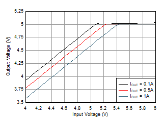
LMR36510 Dropout_LMR36510_5V_22uH.gifFigure 11. Overall Dropout Characteristic
VOUT = 5 V
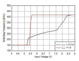
LMR36510 Frequency_Dropout.gifFigure 12. Frequency Dropout Characteristics
ƒSW = 400 kHz