ZHCSO65B January 2023 – January 2024 LMR38020-Q1
PRODUCTION DATA
- 1
- 1 特性
- 2 应用
- 3 说明
- 4 Device Comparison Table
- 5 Pin Configuration and Functions
- 6 Specifications
-
7 Detailed Description
- 7.1 Overview
- 7.2 Functional Block Diagram
- 7.3
Feature Description
- 7.3.1 Fixed Frequency Peak Current Mode Control
- 7.3.2 Adjustable Output Voltage
- 7.3.3 Enable
- 7.3.4 Switching Frequency and Synchronization (RT/SYNC)
- 7.3.5 Power-Good Flag Output
- 7.3.6 Minimum On Time, Minimum Off Time, and Frequency Foldback
- 7.3.7 Bootstrap Voltage
- 7.3.8 Overcurrent and Short Circuit Protection
- 7.3.9 Soft Start
- 7.3.10 Thermal Shutdown
- 7.4 Device Functional Modes
- 8 Application and Implementation
- 9 Device and Documentation Support
- 10Revision History
- 11Mechanical, Packaging, and Orderable Information
8.5.1 Layout Guidelines
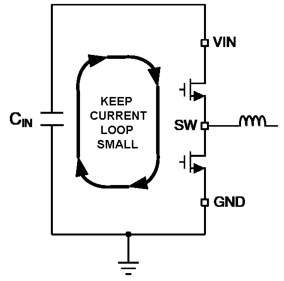
The PCB layout of any DC/DC converter is critical to the optimal performance of the design. Bad PCB layout can disrupt the operation of an otherwise good schematic design. Even if the converter regulates correctly, bad PCB layout can mean the difference between a robust design and one that cannot be mass produced. Furthermore, the EMI performance of the regulator is dependent on the PCB layout, to a great extent. In a buck converter, the most critical PCB feature is the loop formed by the input capacitor or input capacitors, and power ground, as shown in Figure 8-15. This loop carries large transient currents that can cause large transient voltages when reacting with the trace inductance. These unwanted transient voltages disrupt the proper operation of the converter. Because of this, the traces in this loop must be wide and short, and the loop area as small as possible to reduce the parasitic inductance. Figure 8-16 shows a recommended layout for the critical components of the LMR38020-Q1.
- Place the input capacitor or capacitors as close as possible to the VIN and GND terminals. VIN and GND pins are adjacent, simplifying the input capacitor placement.
- Place vias around the input capacitors on the VIN and GND planes. Placing vias reduces the effective inductance and allows for a lower impedance path. Please refer to the evaluation board for guidance.
- Use wide traces for the CBOOT capacitor. Place CBOOT close to the device with short/wide traces to the BOOT and SW pins.
- Place the feedback divider as close as possible to the FB pin of the device. Place RFBB, RFBT, and CFF, if used, physically close to the device. The connections to FB and GND must be short and close to those pins on the device. The connection to VOUT can be somewhat longer. However, this latter trace must not be routed near any noise source (such as the SW node) that can capacitively couple into the feedback path of the regulator.
- Use at least one ground plane in one of the middle layers. This plane acts as a noise shield and also act as a heat dissipation path.
- Connect the thermal pad to the ground plane. The HSOIC package has a thermal pad (PAD) connection that must be soldered down to the PCB ground plane. This pad acts as a heat-sink connection and an electrical ground connection for the regulator. The integrity of this solder connection has a direct bearing on the total effective RθJA of the application.
- Provide wide paths for VIN, VOUT, and GND. Making these paths as wide and direct as possible reduces any voltage drops on the input or output paths of the converter and maximizes efficiency.
- Provide enough PCB area for proper heat sinking. Enough copper area must be used to keep a low RθJA, commensurate with the maximum load current and ambient temperature. Make the top and bottom PCB layers with two-ounce copper; and no less than one ounce. With the SOIC package, use an array of heat-sinking vias to connect the thermal pad (PAD) to the ground plane on the bottom PCB layer. If the PCB design uses multiple copper layers (recommended), thermal vias can also be connected to the inner layer heat-spreading ground planes.
- Keep switch area small. Keep the copper area connecting the SW pin to the inductor as short and wide as possible. At the same time the total area of this node must be minimized to help reduce radiated EMI.
See the following PCB layout resources for additional important guidelines:
- AN-1149 Layout Guidelines for Switching Power Supplies application report
- AN-1229 Simple Switcher® PCB Layout Guidelines application report
- Construction Your Power Supply- Layout Considerations
- Low Radiated EMI Layout Made Simple with LM4360x and LM4600x application report
 Figure 8-15 Current Loops with Fast Edges