ZHCSO65B January 2023 – January 2024 LMR38020-Q1
PRODUCTION DATA
- 1
- 1 特性
- 2 应用
- 3 说明
- 4 Device Comparison Table
- 5 Pin Configuration and Functions
- 6 Specifications
-
7 Detailed Description
- 7.1 Overview
- 7.2 Functional Block Diagram
- 7.3
Feature Description
- 7.3.1 Fixed Frequency Peak Current Mode Control
- 7.3.2 Adjustable Output Voltage
- 7.3.3 Enable
- 7.3.4 Switching Frequency and Synchronization (RT/SYNC)
- 7.3.5 Power-Good Flag Output
- 7.3.6 Minimum On Time, Minimum Off Time, and Frequency Foldback
- 7.3.7 Bootstrap Voltage
- 7.3.8 Overcurrent and Short Circuit Protection
- 7.3.9 Soft Start
- 7.3.10 Thermal Shutdown
- 7.4 Device Functional Modes
- 8 Application and Implementation
- 9 Device and Documentation Support
- 10Revision History
- 11Mechanical, Packaging, and Orderable Information
8.2 Typical Application
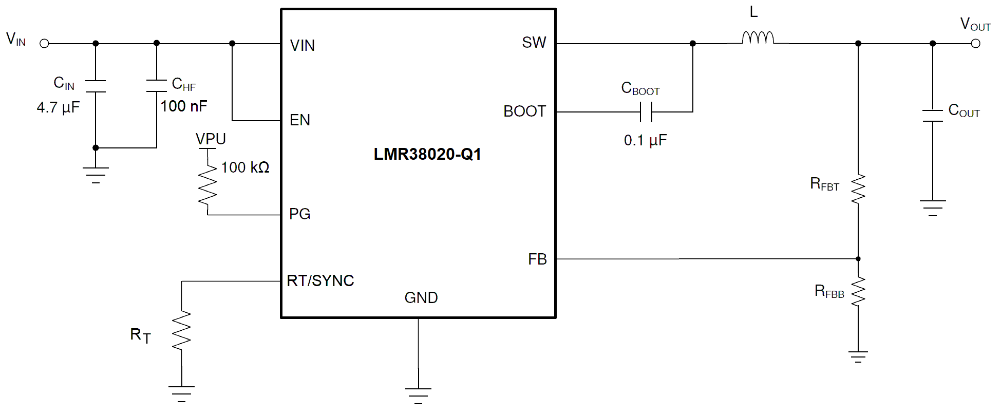
Figure 8-1 shows a typical application circuit for the LMR38020-Q1. This device is designed to function over a wide range of external components and system parameters. However, the internal compensation is optimized for a certain range of external inductance and output capacitance. As a quick-start guide, Table 8-1 provides typical component values for a range of the most common output voltages.
 Figure 8-1 Example Application Circuit
Table 8-1 Typical External Component Values for 2-A Output Current
| ƒSW (kHz) | VIN (V) Typical | VOUT (V) | L (µH) | NOMINAL COUT (RATED CAPACITANCE) | MINIMUM COUT (RATED CAPACITANCE) | RFBT (Ω) | RFBB (Ω) |
|---|---|---|---|---|---|---|---|
| 400 | 48 | 5 | 15 | 3 × 22 µF | 2 × 22 µF | 100 k | 24.9 k |
1000 | 24 | 5 | 6.8 | 2 × 22 µF | 2 × 15 µF | 100 k | 24.9 k |
| 400 | 48 | 12 | 33 | 1× 22 µF | 1 × 15 µF | 100 k | 9.09 k |
1000 | 24 | 12 | 10 | 2 × 10 µF | 1 × 10 µF | 100 k | 9.09 k |
| 500 | 48 | 24 | 47 | 1 × 22 µF | 1 × 15 µF | 100 k | 4.32 k |