ZHCSN38D October   2021  – April 2024 LMR54406 , LMR54410

PRODUCTION DATA  

  1.   1
  2. 特性
  3. 应用
  4. 说明
  5. Device Comparison Table
  6. Pin Configuration and Functions
  7. Specifications
    1. 6.1 Absolute Maximum Ratings
    2. 6.2 ESD Ratings
    3. 6.3 Recommended Operating Conditions
    4. 6.4 Thermal Information
    5. 6.5 Electrical Characteristics
    6. 6.6 Timing Requirements
    7. 6.7 System Characteristics
    8. 6.8 Typical Characteristics
  8. Detailed Description
    1. 7.1 Overview
    2. 7.2 Functional Block Diagram
    3. 7.3 Feature Description
      1. 7.3.1 Fixed Frequency Peak Current Mode Control
      2. 7.3.2 Adjustable Output Voltage
      3. 7.3.3 Enable
      4. 7.3.4 Minimum ON Time, Minimum OFF Time, and Frequency Foldback
      5. 7.3.5 Bootstrap Voltage
      6. 7.3.6 Overcurrent and Short Circuit Protection
      7. 7.3.7 Soft Start
      8. 7.3.8 Thermal Shutdown
    4. 7.4 Device Functional Modes
      1. 7.4.1 Shutdown Mode
      2. 7.4.2 Active Mode
      3. 7.4.3 CCM Mode
      4. 7.4.4 Light Load Operation (PFM Version)
      5. 7.4.5 Light-Load Operation (FPWM Version)
  9. Application and Implementation
    1. 8.1 Application Information
    2. 8.2 Typical Application
      1. 8.2.1 Design Requirements
      2. 8.2.2 Detailed Design Procedure
        1. 8.2.2.1 Output Voltage Set-Point
        2. 8.2.2.2 Switching Frequency
        3. 8.2.2.3 Inductor Selection
        4. 8.2.2.4 Output Capacitor Selection
        5. 8.2.2.5 Input Capacitor Selection
        6. 8.2.2.6 Bootstrap Capacitor
        7. 8.2.2.7 Undervoltage Lockout Set-Point
        8. 8.2.2.8 Replacing Non Sync Converter
      3. 8.2.3 Application Curves
    3. 8.3 Power Supply Recommendations
    4. 8.4 Layout
      1. 8.4.1 Layout Guidelines
        1. 8.4.1.1 Compact Layout for EMI Reduction
        2. 8.4.1.2 Feedback Resistors
      2. 8.4.2 Layout Example
  10. Device and Documentation Support
    1. 9.1 Device Support
      1. 9.1.1 第三方米6体育平台手机版_好二三四免责声明
    2. 9.2 Documentation Support
      1. 9.2.1 Related Documentation
    3. 9.3 接收文档更新通知
    4. 9.4 支持资源
    5. 9.5 Trademarks
    6. 9.6 静电放电警告
    7. 9.7 术语表
  11. 10Revision History
  12. 11Mechanical, Packaging, and Orderable Information

封装选项

机械数据 (封装 | 引脚)
散热焊盘机械数据 (封装 | 引脚)
订购信息

Pin Configuration and Functions

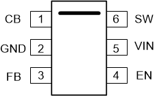
GUID-9C43779C-CEB1-47E4-90AC-0FA7A05F48E8-low.gifFigure 5-1 6-Pin SOT-23DBV Package(Top View)
Table 5-1 Pin Functions
PIN TYPE(1) DESCRIPTION
NAME NO
CB 1 P Bootstrap capacitor connection for high-side FET driver. Connect a high quality 100-nF capacitor from this pin to the SW pin.
GND 2 G Power ground pins. Connected to the source of low-side FET internally. Connect to system ground, ground side of CIN and COUT. The path to CIN must be as short as possible.
FB 3 A Feedback input to the converter. Connect a resistor divider to set the output voltage. Never short this terminal to ground during operation.
EN 4 A Precision enable input to the converter. Do not float. High = on, low = off. Can be tied to VIN. Precision enable input allows an adjustable UVLO by an external resistor divider.
VIN 5 P Supply input pin to the internal bias LDO and high-side FET. Connect to the input supply and input bypass capacitors CIN. Input bypass capacitors must be directly connected to this pin and GND.
SW 6 P Switching output of the converter. Internally connected to source of the high-side FET and drain of the low-side FET. Connect to the power inductor.
A = Analog, P = Power, G = Ground