ZHCSGT2C November 2016 – August 2021 LMS3635-Q1 , LMS3655-Q1
PRODUCTION DATA
- 1 特性
- 2 应用
- 3 说明
- 4 Revision History
- 5 Device Comparison Tables
- 6 Pin Configuration and Functions
- 7 Specifications
- 8 Detailed Description
-
9 Application and Implementation
- 9.1 Application Information
- 9.2
Typical Applications
- 9.2.1
General Application
- 9.2.1.1 Design Requirements
- 9.2.1.2 Detailed Design Procedure
- 9.2.1.3 Application Curves
- 9.2.2 Fixed 5-V Output for USB-Type Applications
- 9.2.3 Fixed 3.3-V Output
- 9.2.4 6-V Adjustable Output
- 9.2.1
General Application
- 9.3 Do's and Don't's
- 10Power Supply Recommendations
- 11Layout
- 12Device and Documentation Support
- 13Mechanical, Packaging, and Orderable Information
8.1 Overview
The LMS36x5-Q1 devices are wide-input voltage range, low quiescent current, high-performance regulators with internal compensation. This device is designed to minimize end-product cost and size while operating in demanding automotive and high-performance industrial environments. Normal operating frequency is 400 kHz, allowing the use of small passive components. This device has a low unloaded current consumption, eliminating the need for an external backup LDO. The LMS36x5-Q1 low shutdown current and high maximum operating voltage also allow for the elimination of an external load switch. To further reduce system cost, an advanced reset output is provided, which can often eliminate the use of an external reset or supervisor device.
The LMS36x5-Q1 is designed with a flip-chip or HotRod™ technology, greatly reducing the parasitic inductance of the pins. In addition, the layout of the device allows for partial cancellation of the current generated magnetic field which reduces the radiated noise generated by the switching action.
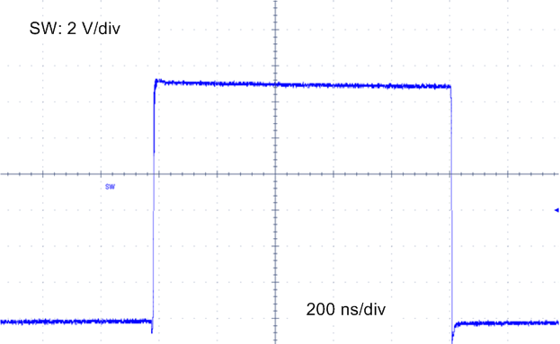
As a result the switch-node waveform exhibits less overshoot and ringing.
 Figure 8-1 Switch Node Waveform (VIN = 13.5 V, IOUT = 5.5 A)
The LMS36x5-Q1 is AEC-Q1-qualified and has electrical characteristics ensured up to a maximum junction temperature of 150°C.
The LMS36x5-Q1 is available in a VQFN package with wettable flanks which allows easy inspection of the soldering without the requirement of x-ray checks.
Throughout this data sheet, references to the LMS3635-Q1 apply equally to the LMS3655-Q1. The difference between the two devices is the maximum output current and specified MOSFET current limits.