ZHCSGY9B July   2017  – March 2018 LMS3655

PRODUCTION DATA.  

  1. 特性
  2. 应用
  3. 说明
    1.     Device Images
      1.      典型应用电路
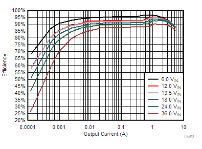
      2.      LMS3655 效率:输出电压 = 5V
  4. 修订历史记录
  5. Device Comparison Table
  6. Pin Configuration and Functions
    1.     Pin Functions
  7. Specifications
    1. 7.1 Absolute Maximum Ratings
    2. 7.2 ESD Ratings
    3. 7.3 Recommended Operating Conditions
    4. 7.4 Thermal Information
    5. 7.5 Thermal Information (for Device Mounted on PCB)
    6. 7.6 Electrical Characteristics
    7. 7.7 System Characteristics
    8. 7.8 Timing Requirements
    9. 7.9 Typical Characteristics
  8. Detailed Description
    1. 8.1 Overview
    2. 8.2 Functional Block Diagram
      1. 8.2.1 Control Scheme
    3. 8.3 Feature Description
      1. 8.3.1 RESET Flag Output
      2. 8.3.2 Enable and Start-Up
      3. 8.3.3 Soft-Start Function
      4. 8.3.4 Current Limit
      5. 8.3.5 Hiccup Mode
      6. 8.3.6 Synchronizing Input
      7. 8.3.7 Undervoltage Lockout (UVLO) and Thermal Shutdown (TSD)
      8. 8.3.8 Input Supply Current
    4. 8.4 Device Functional Modes
      1. 8.4.1 AUTO Mode
      2. 8.4.2 FPWM Mode
      3. 8.4.3 Dropout
      4. 8.4.4 Spread-Spectrum Operation
  9. Application and Implementation
    1. 9.1 Application Information
    2. 9.2 Typical Applications
      1. 9.2.1 General Application
        1. 9.2.1.1 Design Requirements
        2. 9.2.1.2 Detailed Design Procedure
          1. 9.2.1.2.1 External Components Selection
            1. 9.2.1.2.1.1 Input Capacitors
            2. 9.2.1.2.1.2 Output Inductors and Capacitors
              1. 9.2.1.2.1.2.1 Inductor Selection
              2. 9.2.1.2.1.2.2 Output Capacitor Selection
          2. 9.2.1.2.2 FB for Adjustable Output
          3. 9.2.1.2.3 VCC
          4. 9.2.1.2.4 BIAS
          5. 9.2.1.2.5 CBOOT
          6. 9.2.1.2.6 Maximum Ambient Temperature
        3. 9.2.1.3 Application Curves
      2. 9.2.2 Adjustable 5-V Output
        1. 9.2.2.1 Design Requirements
        2. 9.2.2.2 Detailed Design Procedure
        3. 9.2.2.3 Application Curves
      3. 9.2.3 Adjustable 3.3-V Output
        1. 9.2.3.1 Design Requirements
        2. 9.2.3.2 Detailed Design Procedure
        3. 9.2.3.3 Application Curves
      4. 9.2.4 6-V Adjustable Output
        1. 9.2.4.1 Design Requirements
        2. 9.2.4.2 Detailed Design Procedure
        3. 9.2.4.3 Application Curves
    3. 9.3 Do's and Don't's
  10. 10Power Supply Recommendations
  11. 11Layout
    1. 11.1 Layout Guidelines
    2. 11.2 Layout Example
  12. 12器件和文档支持
    1. 12.1 器件支持
      1. 12.1.1 第三方米6体育平台手机版_好二三四免责声明
    2. 12.2 文档支持
      1. 12.2.1 相关文档
    3. 12.3 接收文档更新通知
    4. 12.4 社区资源
    5. 12.5 商标
    6. 12.6 静电放电警告
    7. 12.7 Glossary
  13. 13机械、封装和可订购信息

封装选项

机械数据 (封装 | 引脚)
散热焊盘机械数据 (封装 | 引脚)
订购信息

Application Curves

The following characteristics apply only to the circuit of Figure 35. These parameters are not tested and represent typical performance only. Unless otherwise stated, the following conditions apply: VIN = 12 V, TA = 25°C. For the purpose of offering more information to the designer, information for the application with FPWM pin high (FPWM mode) and FPWM pin low (AUTO mode) is included, although the schematic shows the application running specifically in AUTO mode. The mode is specified under each of the following graphs.
LMS3655 LMS3635-55-tc20-efficiency-auto-snas701.gif
VOUT = 3.3 V AUTO
Figure 36. Efficiency
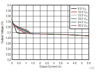
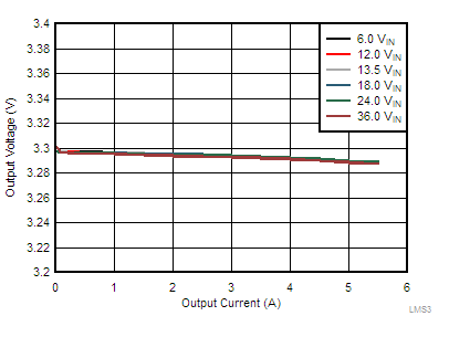
LMS3655 LMS3635-55-tc21-load-and-line-regulation-auto-snas701.gif
VOUT = 3.3 V AUTO
Figure 38. Load and Line Regulation
LMS3655 LMS3635-55-tc25-load-current-for-pfm-to-pwm-transition-snas701.gif
VOUT = 3.3 V
Figure 40. Load Current for PFM-to-PWM Transition
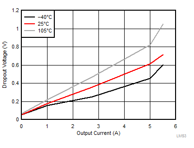
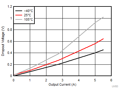
LMS3655 LMS3635-55-tc27-dropout-for-less-than-330khz-snas701.gif
VOUT = 3.3 V
Figure 42. Dropout for ≥ 330 kHz
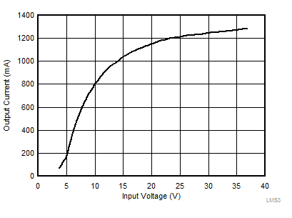
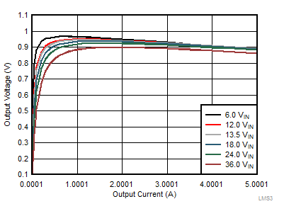
LMS3655 LMS3655-tc19-output-current-level-limit-before-over-current-protection-snas744.gif
VOUT = 3.3 V L = 10 µH
Figure 44. Output Current Level for Overcurrent Protection Trip
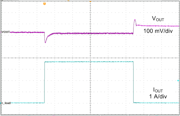
LMS3655 LT-13p5_vin_3p3vout_fpwm.png
FPWM VOUT = 3.3 V L = 10 µH,
COUT = 190 µF IOUT = 0 A to 3.5 A TR = TF = 1 µs
Figure 46. Load Transient
LMS3655 LMS3635-55-tc22-efficiency-fpwm-snas701.gif
VOUT = 3.3 V FPWM
Figure 37. Efficiency
LMS3655 LMS3635-55-tc23-load-and-line-regulation-fpwm-snas701.gif
VOUT = 3.3 V FPWM
Figure 39. Load and Line Regulation
LMS3655 LMS3635-55-tc26-dropout-for-neg-3-percent-regulation-snas701.gif
VOUT = 3.3 V
Figure 41. Dropout for –3% Regulation
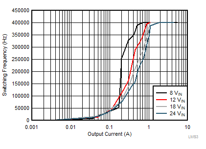
LMS3655 LMS3635-55-tc28-switching-frequency-vs-load-current-snas701.gif
VOUT = 3.3 V AUTO
Figure 43. Switching Frequency vs Load Current
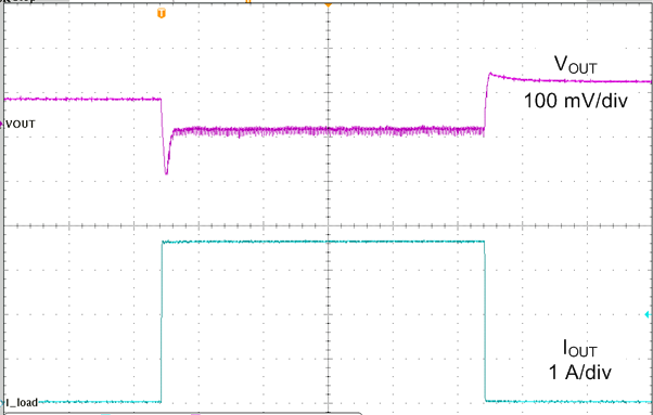
LMS3655 LT-13p5_vin_3p3vout_auto.png
AUTO VOUT = 3.3 V L = 10 µH,
COUT = 190 µF IOUT = 0 A to 3.5 A TR = TF = 1 µs
Figure 45. Load Transient
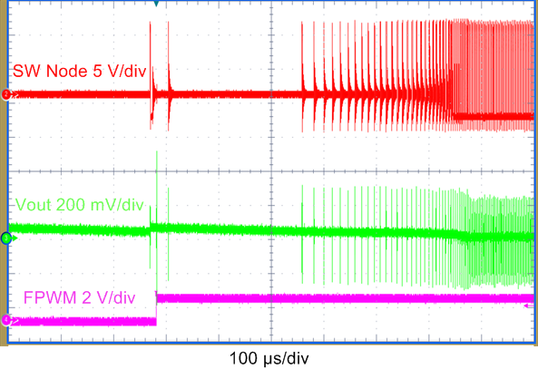
LMS3655 PFM_to_PWM_3p3.png
VOUT = 3.3 V IOUT = 10 mA
Figure 47. Mode Change Transient AUTO to FPWM mode