SNOS487F May 2004 – December 2016 LMS8117A
PRODUCTION DATA.
- 1 Features
- 2 Applications
- 3 Description
- 4 Revision History
- 5 Pin Configuration and Functions
- 6 Specifications
- 7 Detailed Description
- 8 Application and Implementation
- 9 Power Supply Recommendations
- 10Layout
- 11Device and Documentation Support
- 12Mechanical, Packaging, and Orderable Information
封装选项
机械数据 (封装 | 引脚)
散热焊盘机械数据 (封装 | 引脚)
- DCY|4
订购信息
8 Application and Implementation
NOTE
Information in the following applications sections is not part of the TI component specification, and TI does not warrant its accuracy or completeness. TI’s customers are responsible for determining suitability of components for their purposes. Customers should validate and test their design implementation to confirm system functionality.
8.1 Application Information
The LMS8117A is a versatile and high-performance linear regulator with a wide temperature range and tight line and load regulation operation. An output capacitor is required to further improve transient response and stability. For the adjustable version, the ADJUST pin can also be bypassed to achieve very high ripple-rejection ratios. The LMS8117A is versatile in its applications, including uses as a post regulator for DC-DC converters, batter chargers, and microprocessor supplies.
8.2 Typical Applications
8.2.1 Output Regulator
8.2.1.1 Design Requirements
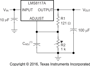
The device component count is very minimal, employing two resistors as part of a voltage divider circuit for the adjustable version and an output capacitor for load regulation. A 10-µF tantalum capacitor on the input is suitable for almost all applications and is required if the regulator is located far from the power-supply filter. An optional bypass capacitor across R2 can also be used to improve PSRR.
8.2.1.2 Detailed Design Procedure
8.2.1.2.1 External Capacitors and Stability
8.2.1.2.1.1 Input Bypass Capacitor
TI recommends an input capacitor. A 10-µF tantalum on the input is a suitable input bypassing for almost all applications.
8.2.1.2.1.2 ADJUST Pin Bypass Capacitor
The ADJUST pin can be bypassed to ground with a bypass capacitor (CADJ) to improve ripple rejection. This bypass capacitor prevents ripple from being amplified as the output voltage is increased. At any ripple frequency, the impedance of the CADJ must be less than R1 to prevent the ripple from being amplified in Equation 1.
The R1 is the resistor between the OUTPUT and the ADJUST pins. Its value is normally from 100 Ω to 200 Ω. For example, with R1 = 124 Ω and fRIPPLE = 120 Hz, the CADJ must be > 11 µF.
8.2.1.2.1.3 Output Capacitor
The output capacitor is critical in maintaining regulator stability, and must meet the required conditions for both minimum amount of capacitance and ESR (Equivalent Series Resistance). The minimum output capacitance required by the LMS8117A is 10 µF, if a tantalum capacitor is used. Any increase of the output capacitance merely improves the loop stability and transient response. The ESR of the output capacitor must be greater than 0.5 Ω and less than 5 Ω. In the case of the adjustable regulator, when the CADJ is used, a larger output capacitance (22-µF tantalum) is required.
8.2.1.2.2 Output Voltage
The LMS8117A adjustable version develops a 1.25-V reference voltage (VREF) between the OUTPUT and the ADJUST pins. As shown in Figure 13, this voltage is applied across resistor R1 to generate a constant current I1. The current IADJ from the ADJUST pin could introduce error to the output. Because it is very small (60 µA) compared with the I1 and very constant with line and load changes, the error can be ignored. The constant current I1 then flows through the output set resistor R2 and sets the output voltage to the desired level.
For fixed voltage devices, R1 and R2 are integrated inside the devices.
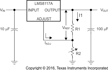 Figure 13. Basic Adjustable Regulator
VOUT is calculated using Equation 2. IADJ is typically 60 µF and negligible in most applications.
8.2.1.2.3 Load Regulation
The LMS8117A regulates the voltage that appears between its OUTPUT and GROUND pins, or between its OUTPUT and ADJUST pins. In some cases, line resistances can introduce errors to the voltage across the load. To obtain the best load regulation, a few precautions are required.
Figure 14 shows a typical application using a fixed output regulator. The RT1 and RT2 are the line resistances. It is obvious that the VLOAD is less than the VOUT by the sum of the voltage drops along the line resistances (as seen in Equation 3). In this case, the load regulation seen at the RLOAD would be degraded from the data sheet specification. To improve this, the load must be tied directly to the OUTPUT pin on the positive side and directly tied to the GROUND pin on the negative side.
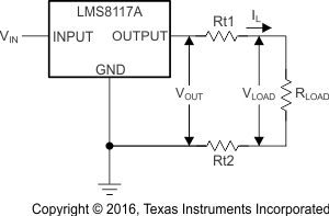 Figure 14. Basic Fixed Output Regulator
When the adjustable regulator is used (Figure 15), the best performance is obtained with the positive side of the resistor R1 tied directly to the OUTPUT pin of the regulator rather than near the load (as seen in Equation 4). This eliminates line drops from appearing effectively in series with the reference and degrading regulation. For example, a 5-V regulator with 0.05-Ω resistance between the regulator and load has a load regulation due to line resistance of 0.05 Ω × IL. If R1 (125 Ω) is connected near the load, the effective line resistance is 0.05 Ω (1 + R2 / R1) or in this case, it is 4 times worse. In addition, the ground side of the resistor R2 can be returned near the ground of the load to provide remote ground sensing and improve load regulation.
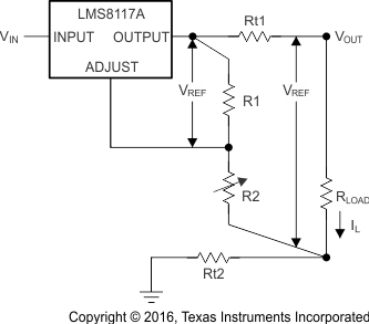 Figure 15. Best Load Regulation Using Adjustable Output Regulator
8.2.1.2.4 Protection Diodes
Under normal operation, the LMS8117A regulators do not require any protection diode. With the adjustable device, the internal resistance between the ADJUST and OUTPUT pins limit the current. No diode is required to divert the current around the regulator even with capacitor on the ADJUST pin. The ADJUST pin can take a transient signal of ±25 V with respect to the output voltage without damaging the device.
When a output capacitor is connected to a regulator and the input is shorted to ground, the output capacitor discharges into the output of the regulator. The discharge current depends on the value of the capacitor, the output voltage of the regulator, and rate of decrease of VIN. In the LMS8117A regulators, the internal diode between the OUTPUT and INPUT pins can withstand microsecond surge currents of 10 A to 20 A. With an extremely large output capacitor (≥1000 µF), and with input instantaneously shorted to ground, the regulator could be damaged.
In this case, TI recommends an external diode between the OUTPUT and INPUT pins to protect the regulator, as shown in Figure 16.
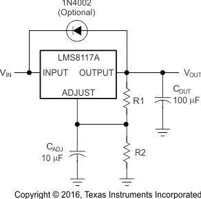 Figure 16. Regulator With Protection Diode
8.2.1.3 Application Curves
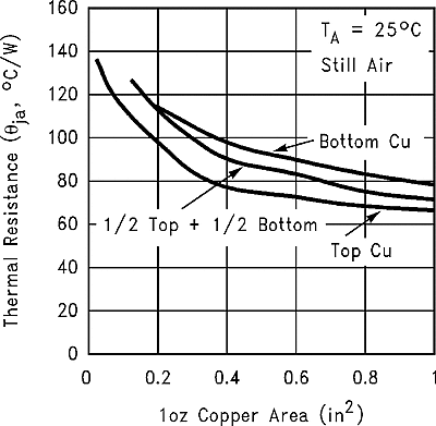
| SOT-223 package |
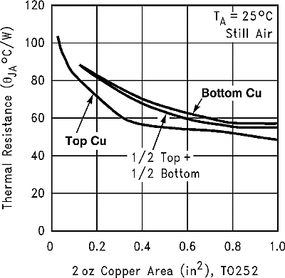
| SOT-223 package |
vs Ambient Temperature
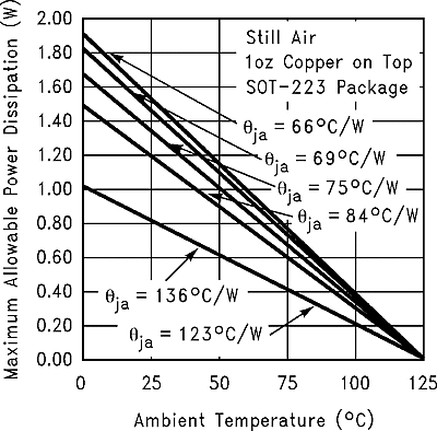
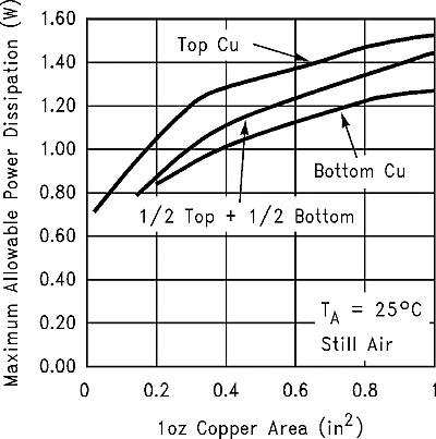
| SOT-223 package |
vs 1-oz Copper Area
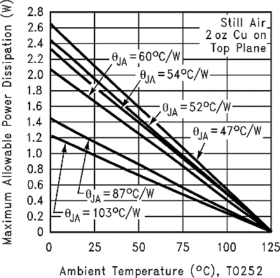
| TO-252 package |
| TO-252 package |
vs Ambient Temperature
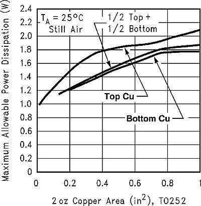
| TO-252 package |
vs 2-oz Copper Area
8.2.2 Other Application Circuits
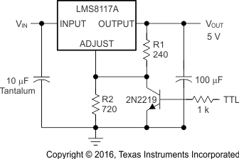
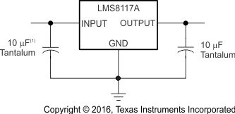
Figure 23 and Figure 24 show application circuit examples using the LMS8117A devices. Customers must fully validate and test any circuit before implementing a design based on an example in this section. Unless otherwise noted, the design procedures in Output Regulator are applicable.
