SNOS487F May 2004 – December 2016 LMS8117A
PRODUCTION DATA.
- 1 Features
- 2 Applications
- 3 Description
- 4 Revision History
- 5 Pin Configuration and Functions
- 6 Specifications
- 7 Detailed Description
- 8 Application and Implementation
- 9 Power Supply Recommendations
- 10Layout
- 11Device and Documentation Support
- 12Mechanical, Packaging, and Orderable Information
封装选项
机械数据 (封装 | 引脚)
散热焊盘机械数据 (封装 | 引脚)
- DCY|4
订购信息
7 Detailed Description
7.1 Overview
The LMS8117A device is a positive-voltage regulator available in 1.8-V, 3.3-V, and adjustable versions. For the adjustable version, the output voltage ranges from 1.25 V to 13.8 V and is set with only two external resistors. This device is capable of supplying up to 1-A output current for an input voltage up to 15 V.
Because this device has a low-dropout voltage of 1.25 V over a junction temperature from 0°C to 125°C, the input voltage can be as low as 2.5 V for proper regulation over the entire temperature range. The LMS8117A also features current limiting and thermal overload protection to help protect the device and is available in the space-saving SOT-223 and TO-252 packages.
The LMS8117A device is versatile in its applications, including uses in programmable output regulation and local on-card regulation. Or, by connecting a fixed resistor between the ADJUST and OUTPUT pins, the device can function as a precision current regulator. An optional output capacitor can be added to improve transient response. The ADJUST pin can be bypassed to achieve very high ripple-rejection ratios, which are difficult to achieve with standard regulators.
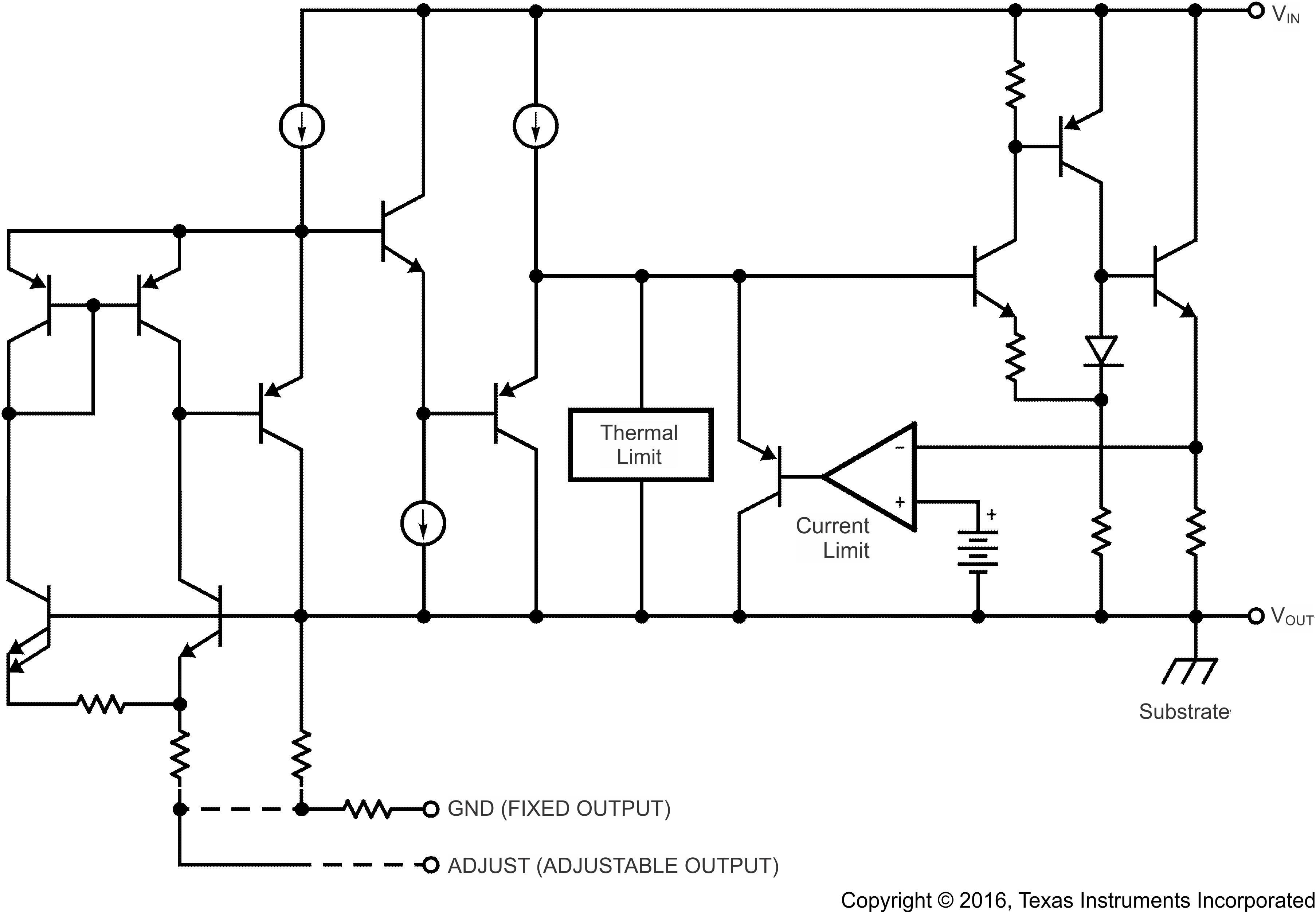
7.2 Functional Block Diagram

7.3 Feature Description
7.3.1 Protection
This device provides current limiting and thermal protection to protect the device against overload or damage from operating in excessive heat.
7.3.2 Programmable Feedback
The ADJUST pin for adjustable versions provide easy output voltage or current (not both) programming. For current regulation applications, a single resistor whose resistance value is 1.25 V/IO and power rating is greater than (1.25 V)2/R must be used. For voltage regulation applications, two resistors set the output voltage.
7.4 Device Functional Modes
7.4.1 Normal Operation
For the adjustable version, the OUTPUT pin sources current as necessary to make VOUT 1.25 V greater than VREF to provide output regulation. For the fixed version, the OUTPUT pin sources current as necessary to make VOUT greater than the GND pin voltage by the specific fixed voltage (version dependent) to provide output regulation.
7.4.2 Operation With Low Input Voltage
The device requires up to 1.25-V headroom (VIN – VOUT) to operate in regulation. With less headroom, the device may dropout and OUTPUT voltage is equal to INPUT voltage minus the dropout voltage.
7.4.3 Operation at Light Loads
The device passes its bias current to the OUTPUT pin. The load or feeedback must consume this minimum current for regulation or the output may be too high.
7.4.4 Operation in Self Protection
When an overload occurs the device will shut down or reduce the output current to prevent device damage. The device will automatically reset from the overload. The output may be reduced or alternate between ON and OFF states until the overload is removed.