SNOS487F May 2004 – December 2016 LMS8117A
PRODUCTION DATA.
- 1 Features
- 2 Applications
- 3 Description
- 4 Revision History
- 5 Pin Configuration and Functions
- 6 Specifications
- 7 Detailed Description
- 8 Application and Implementation
- 9 Power Supply Recommendations
- 10Layout
- 11Device and Documentation Support
- 12Mechanical, Packaging, and Orderable Information
封装选项
机械数据 (封装 | 引脚)
散热焊盘机械数据 (封装 | 引脚)
- DCY|4
订购信息
10 Layout
10.1 Layout Guidelines
- TI recommends bypassing the input pin to ground with a bypass capacitor.
- The optimum placement of the bypass capacitor is as close as possible to the input pin and the system ground. Take care to minimize the loop area formed by the bypass capacitor connection, the input pin, and the system GND.
- TI recommends using wide trace lengths to eliminate I × R drop and heat dissipation.
10.2 Layout Example
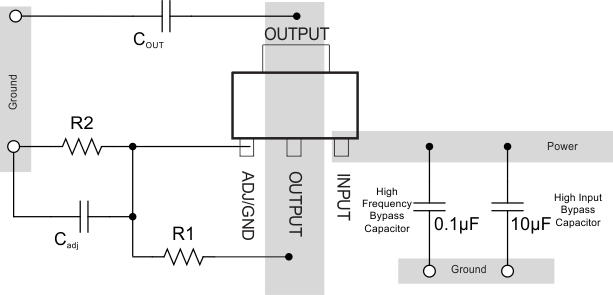 Figure 25. SOT-223 Layout Example for LMS8117A Adjustable Version (Schematic View)
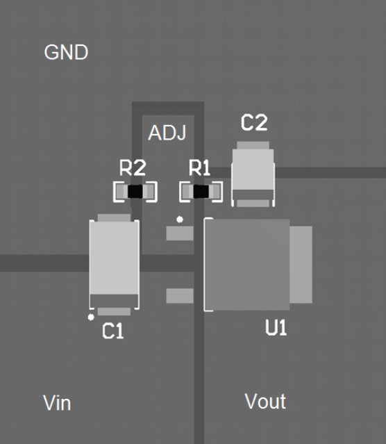 Figure 26. TO-252 Layout Example for LMS8117A Adjustable Version (PCB View)
10.3 Thermal Considerations
10.3.1 Heat Sink Requirements
When an integrated circuit operates with an appreciable current, its junction temperature is elevated. It is important to quantify its thermal limits to achieve acceptable performance and reliability. This limit is determined by summing the individual parts consisting of a series of temperature rises from the semiconductor junction to the operating environment. A one-dimensional steady-state model of conduction heat transfer is demonstrated in Figure 27. The heat generated at the device junction flows through the die to the die attach pad, through the lead frame to the surrounding case material, to the printed-circuit board, and eventually to the ambient environment.
There are several variables that may affect the thermal resistance and in turn the need for a heat sink, which include the following.
Component variables (RθJC)
- Leadframe size and material
- Number of conduction pins
- Die size
- Die attach material
- Molding compound size and material
Application variables (RθCA)
- Mounting pad size, material, and location
- Placement of mounting pad
- PCB size and material
- Traces length and width
- Adjacent heat sources
- Volume of air
- Ambient temperature
- Shape of mounting pad

The LMS8117A regulator has internal thermal shutdown to protect the device from overheating. Under all possible operating conditions, the junction temperature of the LMS8117A must be within 0°C to 125°C. A heat sink may be required depending on the maximum power dissipation and maximum ambient temperature of the application. To determine if a heat sink is required, the power dissipated by the regulator (PD) is calculated using Equation 6.
Figure 28 shows the voltages and currents which are present in the circuit.
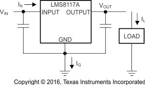 Figure 28. Power Dissipation Diagram
The next parameter which must be calculated is the maximum allowable temperature rise (TR(MAX)) in Equation 8.
where
- TJ(MAX) is the maximum allowable junction temperature (125°C)
- TA(MAX) is the maximum ambient temperature encountered in the application
Using the calculated values for TR(MAX) and PD, the maximum allowable value for the junction-to-ambient thermal resistance (RθJA) can be calculated with Equation 9.
If the maximum allowable value for RθJA is found to be ≥61.4°C/W for SOT-223 package or ≥56.1°C/W for
TO-252 package, no heat sink is required because the package alone dissipates enough heat to satisfy these requirements. If the calculated value for RθJA falls below these limits, a heat sink is required.
As a design aid, Table 1 shows the value of the RθJA of SOT-223 and TO-252 for different heat sink area. The copper patterns that we used to measure these RθJA are shown Figure 29 and Figure 30. Figure 17 and Figure 18 reflect the same test results as what are in the Table 1.
Figure 19 and Figure 20 show the maximum allowable power dissipation versus ambient temperature for the SOT-223 and TO-252 device packages. Figure 21 and Figure 22 show the maximum allowable power dissipation versus copper area (in.2) for the SOT-223 and TO-252 device packages. For power enhancement techniques to be used with SOT-223 and TO-252 packages, see AN–1028 Maximum Power Enhancement Techniques for Power Packages (SNVA036).
Table 1. RθJA Different Heat Sink Area
| LAYOUT | COPPER AREA (in2) | THERMAL RESISTANCE: RθJA (°C/W) | ||
|---|---|---|---|---|
| TOP SIDE(1) | BOTTOM SIDE | SOT-223 | T0-252 | |
| 1 | 0.0123 | 0 | 136 | 103 |
| 2 | 0.066 | 0 | 123 | 87 |
| 3 | 0.3 | 0 | 84 | 60 |
| 4 | 0.53 | 0 | 75 | 54 |
| 5 | 0.76 | 0 | 96 | 52 |
| 6 | 1 | 0 | 66 | 47 |
| 7 | 0 | 0.2 | 115 | 64 |
| 8 | 0 | 0.4 | 98 | 70 |
| 9 | 0 | 0.6 | 89 | 63 |
| 10 | 0 | 0.8 | 82 | 57 |
| 11 | 0 | 1 | 79 | 57 |
| 12 | 0.066 | 0.066 | 125 | 89 |
| 13 | 0.175 | 0.175 | 93 | 72 |
| 14 | 0.284 | 0.284 | 83 | 61 |
| 15 | 0.392 | 0.392 | 75 | 55 |
| 16 | 0.5 | 0.5 | 70 | 53 |
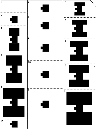 Figure 29. Top View of the Thermal Test Pattern in Actual Scale
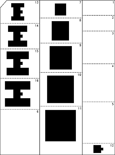 Figure 30. Bottom View of the Thermal Test Pattern in Actual Scale