SNOS487F May 2004 – December 2016 LMS8117A
PRODUCTION DATA.
- 1 Features
- 2 Applications
- 3 Description
- 4 Revision History
- 5 Pin Configuration and Functions
- 6 Specifications
- 7 Detailed Description
- 8 Application and Implementation
- 9 Power Supply Recommendations
- 10Layout
- 11Device and Documentation Support
- 12Mechanical, Packaging, and Orderable Information
封装选项
机械数据 (封装 | 引脚)
散热焊盘机械数据 (封装 | 引脚)
- DCY|4
订购信息
6 Specifications
6.1 Absolute Maximum Ratings
over operating free-air temperature range (unless otherwise noted)(1)(2)| MIN | MAX | UNIT | ||
|---|---|---|---|---|
| Maximum input voltage (all versions), VIN | 20 | V | ||
| Power dissipation(3) | Internally limited | |||
| Junction temperature, TJ(MAX) | 150 | °C | ||
| Storage temperature, Tstg | –65 | 150 | °C | |
(1) Stresses beyond those listed under Absolute Maximum Ratings may cause permanent damage to the device. These are stress ratings only, which do not imply functional operation of the device at these or any other conditions beyond those indicated under Recommended Operating Conditions. Exposure to absolute-maximum-rated conditions for extended periods may affect device reliability.
(2) If Military/Aerospace specified devices are required, please contact the Texas Instruments Sales Office/Distributors for availability and specifications.
(3) The maximum power disspation is a function of TJ(MAX), RθJA, and TA. The maximum allowable power dissipation at any ambient temperature is PD = (TJ(MAX) – TA) / RθJA. All numbers apply for packages soldered directly onto a PCB.
6.2 ESD Ratings
| VALUE | UNIT | |||
|---|---|---|---|---|
| V(ESD) | Electrostatic discharge | Human-body model (HBM), per ANSI/ESDA/JEDEC JS-001(1)(2) | ±2000 | V |
(1) JEDEC document JEP155 states that 500-V HBM allows safe manufacturing with a standard ESD control process.
(2) For testing purposes, ESD was applied using human body model, 1.5-kΩ resistor in series iwth 100-pF capacitor.
6.3 Recommended Operating Conditions
over operating free-air temperature range (unless otherwise noted)| MIN | MAX | UNIT | ||
|---|---|---|---|---|
| Input voltage (all versions) | 15 | V | ||
| Junction temperature, TJ | 0 | 125 | °C | |
6.4 Thermal Information
| THERMAL METRIC(1) | LMS8117A | UNIT | ||
|---|---|---|---|---|
| DCY (SOT-223) | NDP (TO-252) | |||
| 4 PINS | 3 PINS | |||
| RθJA | Junction-to-ambient thermal resistance | 61.4 | 56.1 | °C/W |
| RθJC(top) | Junction-to-case (top) thermal resistance | 43 | 42.8 | °C/W |
| RθJB | Junction-to-board thermal resistance | 10 | 29.4 | °C/W |
| ψJT | Junction-to-top characterization parameter | 2.4 | 5.4 | °C/W |
| ψJB | Junction-to-board characterization parameter | 9.9 | 28.9 | °C/W |
| RθJC(bot) | Junction-to-case (bottom) thermal resistance | — | 4.1 | °C/W |
(1) For more information about traditional and new thermal metrics, see the Semiconductor and IC Package Thermal Metrics application report.
6.5 Electrical Characteristics
Typical values apply for TJ = 25°C and Minimum and Maximum limits apply for TJ = 0°C to 125°C (unless otherwise noted). Typical values represent the most likely parametric norm. All limits are guaranteed using by testing or statistical analysis.| PARAMETER | TEST CONDITIONS | MIN | TYP | MAX | UNIT | ||
|---|---|---|---|---|---|---|---|
| VREF | Reference voltage | Adjustable version | IOUT = 10 mA, VIN – VOUT = 2 V, TJ = 25°C | 1.238 | 1.25 | 1.262 | V |
| IOUT = 10 mA to 1 A, VIN – VOUT = 1.4 V to 10 V | 1.225 | 1.27 | |||||
| VOUT | Output voltage | 1.8-V version | IOUT = 10 mA, VIN = 3.8 V, TJ = 25°C | 1.782 | 1.8 | 1.818 | V |
| IOUT = 0 A to 1 A, VIN = 3.2 V to 10 V | 1.746 | 1.854 | |||||
| 3.3-V version | IOUT = 10 mA, VIN = 5 V, TJ = 25°C | 3.267 | 3.3 | 3.333 | |||
| IOUT = 0 A to 1 A, VIN = 4.75 V to 10 V | 3.235 | 3.365 | |||||
| ΔVOUT | Line regulation(1) | Adjustable version, IOUT = 10 mA, VIN – VOUT = 1.5 V to 13.75 V | 0.035% | 0.2% | |||
| 1.8-V version, IOUT = 0 mA, VIN = 3.2 V to 10 V | 1 | 6 | mV | ||||
| 3.3-V version, IOUT = 0 mA , VIN = 4.75 V to 15 V | 1 | 6 | |||||
| Load regulation(1) | Adjustable version, IOUT = 10 mA to 1 A, VIN – VOUT = 3 V | 0.2% | 0.4% | ||||
| 1.8-V version, IOUT = 0 mA to 1 A, VIN = 3.2 V | 1 | 10 | mV | ||||
| 3.3-V version, IOUT = 0 mA to 1 A, VIN = 4.75 V | 1 | 10 | |||||
| VIN – VOUT | Dropout voltage(2) | IOUT = 100 mA | 1.1 | 1.15 | V | ||
| IOUT = 500 mA | 1.15 | 1.2 | |||||
| IOUT = 1 A | 1.1 | 1.25 | |||||
| ILIMIT | Current limit | VIN – VOUT = 5 V, TJ = 25°C | 1 | 1.4 | 1.9 | A | |
| Minimum load current(3) | Adjustable version, VIN = 15 V | 1.7 | 5 | mA | |||
| Quiescent current | 1.8-V and 3.3-V versions, VIN ≤ 15 V | 5 | 10 | mA | |||
| Thermal regulation | 30-ms pulse, TA = 25°C | 0.01% | 0.1% | W | |||
| Ripple regulation | fRIPPLE = 120 Hz, VIN – VOUT = 3 V, VRIPPLE = 1 VPP | 60 | 75 | dB | |||
| ADJUST pin current | 60 | 120 | µA | ||||
| ADJUST pin current change | IOUT = 10 mA to 1 A, VIN – VOUT = 1.4 V to 10 V | 0.2 | 5 | µA | |||
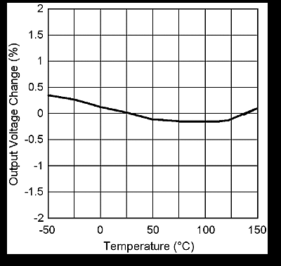
| Temperature stability | 0.5% | ||||||
| Long term stability | 1000 hrs, TA = 125°C | 0.3% | |||||
| RMS output noise | Percentage of VOUT, f = 10 Hz to 10 kHz | 0.003% | |||||
(1) Line and load regulation are measured at constant junction room temperature.
(2) The dropout voltage is the input and output differential at which the circuit ceases to regulate against further reduction in input voltage. It is measured when the output voltage drops 100 mV from the nominal value obtained by VIN = VOUT + 1.5 V.
(3) The minimum output current required to maintain regulation.
6.6 Typical Characteristics
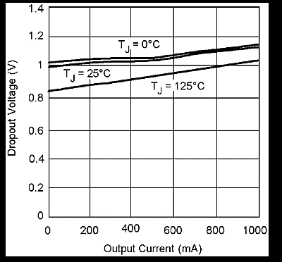 Figure 1. Dropout Voltage
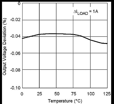
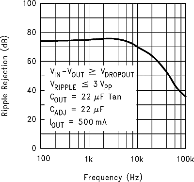
| Adjustable version |
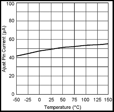
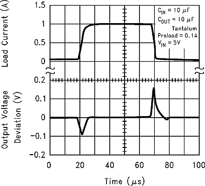
| 3.3 V version |
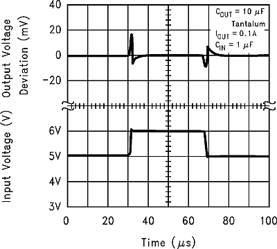
| 3.3 V version |
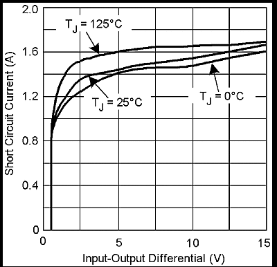 Figure 2. Short-Circuit Current
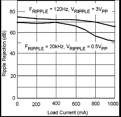
| Adjustable version |
| 1.8 V version |
| 1.8 V version |