SLOS447I September 2004 – May 2016 LMV341 , LMV342 , LMV344
PRODUCTION DATA.
- 1 Features
- 2 Applications
- 3 Description
- 4 Revision History
- 5 Pin Configuration and Functions
- 6 Specifications
- 7 Detailed Description
- 8 Application and Implementation
- 9 Power Supply Recommendations
- 10Layout
- 11Device and Documentation Support
- 12Mechanical, Packaging, and Orderable Information
封装选项
请参考 PDF 数据表获取器件具体的封装图。
机械数据 (封装 | 引脚)
- D|8
- DGK|8
散热焊盘机械数据 (封装 | 引脚)
订购信息
8 Application and Implementation
NOTE
Information in the following applications sections is not part of the TI component specification, and TI does not warrant its accuracy or completeness. TI’s customers are responsible for determining suitability of components for their purposes. Customers should validate and test their design implementation to confirm system functionality.
8.1 Application Information
LMV34x devices have rail-to-rail output and input range from ground to VCC – 1 V. CMOS inputs provide very low input current. Shutdown capability is an option in dual amplifier version. Operation from 2.5-V to 5.5-V is possible.
8.2 Typical Application
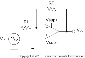
A typical application for an operational amplifier in an inverting amplifier. This amplifier takes a positive voltage on the input, and makes it a negative voltage of the same magnitude. In the same manner, it also makes negative voltages positive.
 Figure 37. Application Schematic
8.2.1 Design Requirements
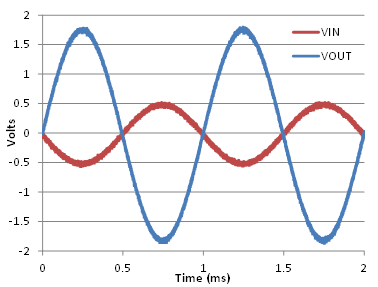
The supply voltage must be chosen such that it is larger than the input voltage range and output range. For instance, this application scales a signal of ±0.5 V to ±1.8 V. Setting the supply at ± 2 V is sufficient to accommodate this application. The supplies can power up in any order; however, neither supply can be of opposite polarity relative to ground at any time; otherwise, a large current can flow though the input ESD diodes. To limit current in such an occurrence, TI highly recommends adding a series resistor to the grounded input. Vsup+ must be more positive than Vsup– at all times; otherwise, a large reverse supply current may flow.
8.2.2 Detailed Design Procedure
Determine the gain required by the inverting amplifier using Equation 1 and Equation 2.


Once the desired gain is determined, choose a value for RI or RF. Choosing a value in the kΩ range is desirable because the amplifier circuit uses currents in the mA range. This ensures the part does not draw too much current. For this example, choose 10 kΩ for RI, which means 36 kΩ is used for RF. This was determined by Equation 3.

8.2.3 Application Curve
 Figure 38. Input and Output Voltages of the Inverting Amplifier