SLOS447I September 2004 – May 2016 LMV341 , LMV342 , LMV344
PRODUCTION DATA.
- 1 Features
- 2 Applications
- 3 Description
- 4 Revision History
- 5 Pin Configuration and Functions
- 6 Specifications
- 7 Detailed Description
- 8 Application and Implementation
- 9 Power Supply Recommendations
- 10Layout
- 11Device and Documentation Support
- 12Mechanical, Packaging, and Orderable Information
封装选项
请参考 PDF 数据表获取器件具体的封装图。
机械数据 (封装 | 引脚)
- D|14
- PW|14
散热焊盘机械数据 (封装 | 引脚)
订购信息
7 Detailed Description
7.1 Overview
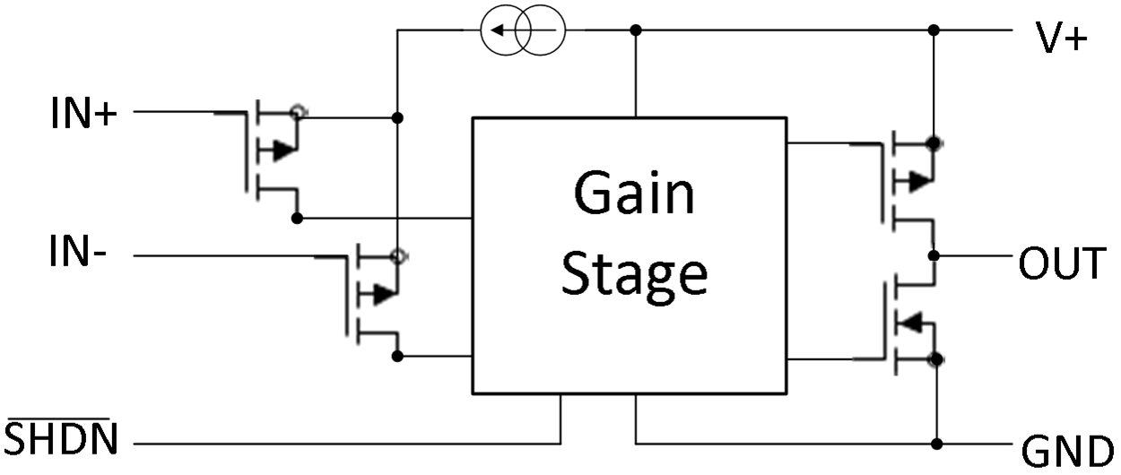
The LMV34x devices are precision operational amplifiers with CMOS inputs for very low input bias current. Output is rail-to-rail and input common-mode includes ground. LMV341 has a shutdown mode for very low supply current.
7.2 Functional Block Diagram

7.3 Feature Description
7.3.1 PMOS Input Stage
PMOS Input Stage supports a lower input range that includes ground. Upper range limit is V+ – 1 V.
7.3.2 CMOS Output Stage
The CMOS drain output topology allows rail-to-rail output swing.
7.3.3 Shutdown
LMV341 includes a shutdown pin. During shutdown, ICC is nearly zero and the output becomes high impedance. The typical turnon time coming out of shutdown is 5 µs.
7.4 Device Functional Modes
The LMV34x devices have two modes of operation:
- Normal operation when SHDN pin is at V+ level or the SHDN pin is not present
- Shutdown mode when SHDN is at GND level; ICC is very low and output is high impedance.