SNOS519K April 2000 – August 2016 LMV710-N
PRODUCTION DATA.
- 1 Features
- 2 Applications
- 3 Description
- 4 Revision History
- 5 Pin Configuration and Functions
- 6 Specifications
- 7 Detailed Description
- 8 Application and Implementation
- 9 Power Supply Recommendations
- 10Layout
- 11Device and Documentation Support
- 12Mechanical, Packaging, and Orderable Information
7 Detailed Description
7.1 Overview
The LMV710-N, LMV711-N, and LMV715-N operational amplifiers provide a CMOS input stage, high current drive rail-to-rail output, and a greater than RR input common mode voltage range. They also provide a slew rate of 5 V/µs at a bandwidth of 5 MHz.
7.2 Functional Block Diagram
7.3 Feature Description
7.3.1 Supply Bypassing
The application circuits in this datasheet do not show the power supply connections and the associated bypass capacitors for simplification. When the circuits are built, it is always required to have bypass capacitors. Ceramic disc capacitors (0.1 µF) or solid tantalum (1 µF) with short leads, and located close to the IC are usually necessary to prevent interstage coupling through the power supply internal impedance. Inadequate bypassing will manifest itself by a low frequency oscillation or by high frequency instabilities. Sometimes, a 10-µF (or larger) capacitor is used to absorb low frequency variations and a smaller 0.1-µF disc is paralleled across it to prevent any high frequency feedback through the power supply lines.
7.3.2 Shutdown Mode
The LMV711 and LMV715 have a shutdown pin. To conserve battery life in portable applications, they can be disabled when the shutdown pin voltage is pulled low. For LMV711 during shutdown mode, the output stays at about 50 mV from the lower rail, and the current drawn from the power supply is 0.2 µA (typical). This makes the LMV711 an ideal solution for power sensitive applications. For the LMV715 during shutdown mode, the output is tri-stated.
The shutdown pin must never be left unconnected. In applications where shutdown operation is not required and the LMV711 or LMV715 is used, the shutdown pin must be connected to V+. Leaving the shutdown pin floating results in an undefined operation mode and the device may oscillate between shutdown and active modes.
7.3.3 Rail-to-Rail Input
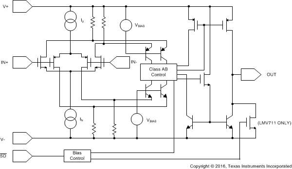
The rail-to-rail input is achieved by using paralleled PMOS and NMOS differential input stages (see Functional Block Diagram). When the common mode input voltage changes from ground to the positive rail, the input stage goes through three modes. First, the NMOS pair is cutoff and the PMOS pair is active. At around 1.4 V, both PMOS and NMOS pairs operate, and finally the PMOS pair is cutoff and NMOS pair is active. Because both input stages have their own offset voltage (VOS), the offset of the amplifier becomes a function of the common-mode input voltage (see Figure 33 and Figure 34 in Typical Characteristics).
As shown in the curve, the VOS has a crossover point at 1.4 V above V–. Proper design must be done in both DC- and AC-coupled applications to avoid problems. For large input signals that include the VOS crossover point in their dynamic range, it causes distortion in the output signal. One way to avoid such distortion is to keep the signal away from the crossover point. For example, in a unity-gain buffer configuration and with VS = 5 V, a 3-V peak-to-peak signal center at 2.5 V contains input-crossover distortion. To avoid this, the input signal must be centered at 3.5 V instead. Another way to avoid large signal distortion is to use a gain of −1 circuit which avoids any voltage excursions at the input terminals of the amplifier (see Figure 35). In this circuit, the common-mode DC voltage (VCM) can be set at a level away from the VOS crossover point.
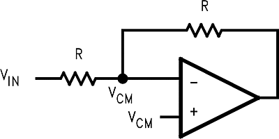 Figure 35. Inverting Configuration
When the input is a small signal and this small signal falls inside the VOS transition range, the gain, CMRR and some other parameters is degraded. To resolve this problem, the small signal must be placed such that it avoids the VOS crossover point.
To achieve maximum output swing, the output must be biased at mid-supply. This is normally done by biasing the input at mid-supply. But with supply voltage range from 2 V to 3.4 V, the input of the op amp must not be biased at mid-supply because of the transition of the VOS. Figure 36 shows an example of how to get away from the VOS crossover point and maintain a maximum swing with a 2.7-V supply. Figure 37 shows the waveforms of VIN and VOUT.
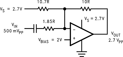 Figure 36. Vout biasing Example
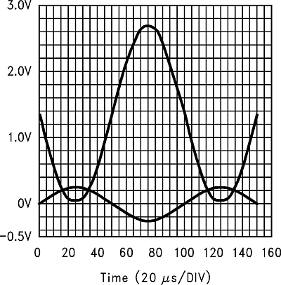 Figure 37. Vout biasing Output Results
The inputs can be driven 300 mV beyond the supply rails without causing phase reversal at the output. However, the inputs must not be allowed to exceed the maximum ratings.
7.4 Device Functional Modes
7.4.1 Compensation of Input Capacitance
In the application (Figure 38) where a large feedback resistor is used, the feedback resistor can react with the input capacitance of the op amp and introduce an additional pole to the close loop frequency response.
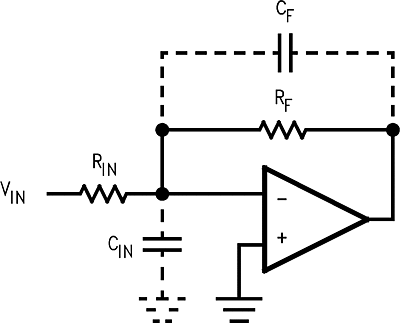 Figure 38. Cancelling the Effect of Input Capacitance
This pole occurs at frequency fp with Equation 1.

Any stray capacitance due to external circuit board layout, any source capacitance from transducer or photodiode connected to the summing node is added to the input capacitance. If fp is less than or close to the unity-gain bandwidth (5 MHz) of the op amp, the phase margin of the loop is reduced and can cause the system to be unstable.
To avoid this problem, make sure that fp occurs at least 2 octaves beyond the expected −3 dB frequency corner of the close loop frequency response. If not, a feedback capacitor CF can be placed in parallel with RF such that Equation 2.

The paralleled RF and CF introduce a zero, which cancels the effect from the pole.
7.4.2 Capacitive Load Tolerance
The LMV71x-N can directly drive 200 pF in unity-gain without oscillation. The unity-gain follower is the most sensitive configuration to capacitive loading. Direct capacitive loading reduces the phase margin of amplifiers. The combination of the amplifier's output impedance and the capacitive load induces phase lag. This results in either an underdamped pulse response or oscillation. To drive a heavier capacitive load, circuit in Figure 39 can be used.
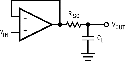 Figure 39. Indirectly Driving a Capacitive Load Using Resistive Isolation
In Figure 39, the isolation resistor RISO and the load capacitor CL form a pole to increase stability by adding more phase margin to the overall system. The desired performance depends on the value of RISO. The bigger the RISO resistor value, the more stable VOUT is. But the DC accuracy is not great when the RISO gets bigger. If there were a load resistor in Figure 39, the output would be voltage divided by RISO and the load resistor.
The circuit in Figure 40 is an improvement to the one in Figure 39 because it provides DC accuracy as well as AC stability. In this circuit, RF provides the DC accuracy by using feed-forward techniques to connect VIN to RL. CF and RISO serve to counteract the loss of phase margin by feeding the high-frequency component of the output signal back to the inverting input of the amplifier, thereby preserving phase margin in the overall feedback loop. Increased capacitive drive is possible by increasing the value of CF . This in turn slows down the pulse response.
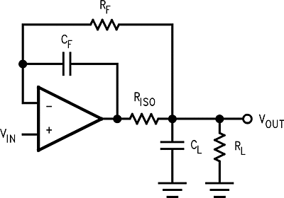 Figure 40. Indirectly Driving a Capacitive a Load With DC Accuracy