SNOS519K April   2000  – August 2016 LMV710-N

PRODUCTION DATA.  

  1. Features
  2. Applications
  3. Description
  4. Revision History
  5. Pin Configuration and Functions
  6. Specifications
    1. 6.1 Absolute Maximum Ratings
    2. 6.2 ESD Ratings
    3. 6.3 Recommended Operating Conditions
    4. 6.4 Thermal Information
    5. 6.5 Electrical Characteristics - 2.7 V
    6. 6.6 Electrical Characteristics - 3.2 V
    7. 6.7 Electrical Characteristics - 5 V
    8. 6.8 Typical Characteristics
  7. Detailed Description
    1. 7.1 Overview
    2. 7.2 Functional Block Diagram
    3. 7.3 Feature Description
      1. 7.3.1 Supply Bypassing
      2. 7.3.2 Shutdown Mode
      3. 7.3.3 Rail-to-Rail Input
    4. 7.4 Device Functional Modes
      1. 7.4.1 Compensation of Input Capacitance
      2. 7.4.2 Capacitive Load Tolerance
  8. Application and Implementation
    1. 8.1 Application Information
    2. 8.2 Typical Applications
      1. 8.2.1 High-Side Current-Sensing
        1. 8.2.1.1 Design Requirements
        2. 8.2.1.2 Detailed Design Procedure
        3. 8.2.1.3 Application Curve
      2. 8.2.2 Peak Detector
        1. 8.2.2.1 Design Requirements
        2. 8.2.2.2 Detailed Design Procedure
      3. 8.2.3 GSM Power Amplifier Control Loop
        1. 8.2.3.1 Design Requirements
        2. 8.2.3.2 Detailed Design Procedure
  9. Power Supply Recommendations
  10. 10Layout
    1. 10.1 Layout Guidelines
    2. 10.2 Layout Example
  11. 11Device and Documentation Support
    1. 11.1 Device Support
      1. 11.1.1 Development Support
    2. 11.2 Documentation Support
      1. 11.2.1 Related Documentation
    3. 11.3 Related Links
    4. 11.4 Receiving Notification of Documentation Updates
    5. 11.5 Community Resources
    6. 11.6 Trademarks
    7. 11.7 Electrostatic Discharge Caution
    8. 11.8 Glossary
  12. 12Mechanical, Packaging, and Orderable Information

封装选项

机械数据 (封装 | 引脚)
散热焊盘机械数据 (封装 | 引脚)
订购信息

5 Pin Configuration and Functions

LMV710 DBV Package
5-Pin SOT-23
Top View
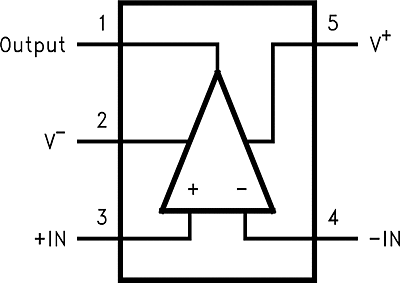
LMV710-N LMV711-N LMV715-N 10132514.gif
LMV711, LMV715 DBV Package
6-Pin SOT-23
Top View
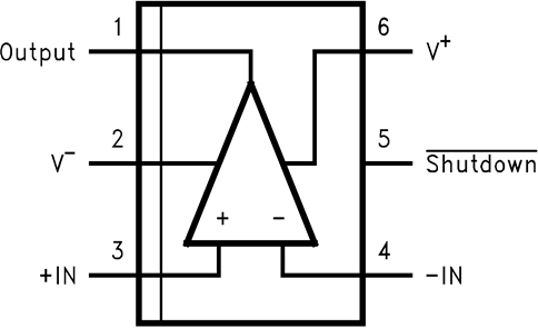
LMV710-N LMV711-N LMV715-N 10132515.png

Pin Functions

PIN TYPE(1) DESCRIPTION
NAME DBV (5) DBV (6)
+IN 3 3 I Noninverting input
–IN 4 4 I Inverting input
Output 1 1 O Output
Shutdown 5 I Active low enable input
V+ 5 6 P Positive supply input
V 2 2 P Supply negative input
(1) I = Input, O = Output, P = Power