SNOS458I April 2000 – June 2016 LMV7219
PRODUCTION DATA.
8 Application and Implementation
NOTE
Information in the following applications sections is not part of the TI component specification, and TI does not warrant its accuracy or completeness. TI’s customers are responsible for determining suitability of components for their purposes. Customers should validate and test their design implementation to confirm system functionality.
8.1 Application Information
The following section explains in detail how to manipulate the hysteresis voltage of the LMV7219. Detailed expressions are provided along with practical considerations for designing hysteresis.
8.2 Typical Application
Figure 14 shows the typical method of adding external hysteresis to a comparator. The positive feedback is responsible for shifting the comparator trip point depending on the state of the output.
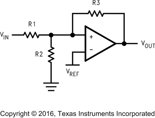 Figure 14. Additional Hysteresis
8.2.1 Design Requirements
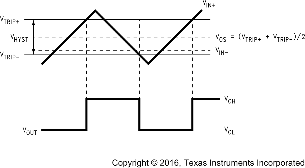
The internal hysteresis creates two trip points, one for the rising input voltage and one for the falling input voltage, as shown in Figure 19. The difference between the trip points is the hysteresis. With internal hysteresis, when the comparator's input voltages are equal, the hysteresis effectively causes one comparator-input voltage to move quickly past the other, thus taking the input out of the region where oscillation occurs. Standard comparators require hysteresis to be added with external resistors. The fixed internal hysteresis eliminates these resistors.
8.2.2 Detailed Design Procedure
8.2.2.1 Additional Hysteresis
If additional hysteresis is desired, this can be done with the addition of three resistors using positive feedback, as shown in Figure 14. The positive feedback method slows the comparator response time. Calculate the resistor values as follows:
1. Select R3. The current through R3 should be greater than the input bias current to minimize errors. The current through R3 (IF) at the trip point is (VREF - VOUT) /R3. Consider the two possible output states when solving for R3, and use the smaller of the two resulting resistor values. The two formulas are:
When VOUT = 0:
When VOUT = VCC:
2. Choose a hysteresis band required (VHB).
3. Calculate R1, where R1 = R3 X(VHB/VCC)
4. Choose the trip point for VIN rising. This is the threshold voltage (VTHR) at which the comparator switches from low to high as VIN rises about the trip point.
5. Calculate R2 as follows:

6. Verify the trip voltage and hysteresis as follows:
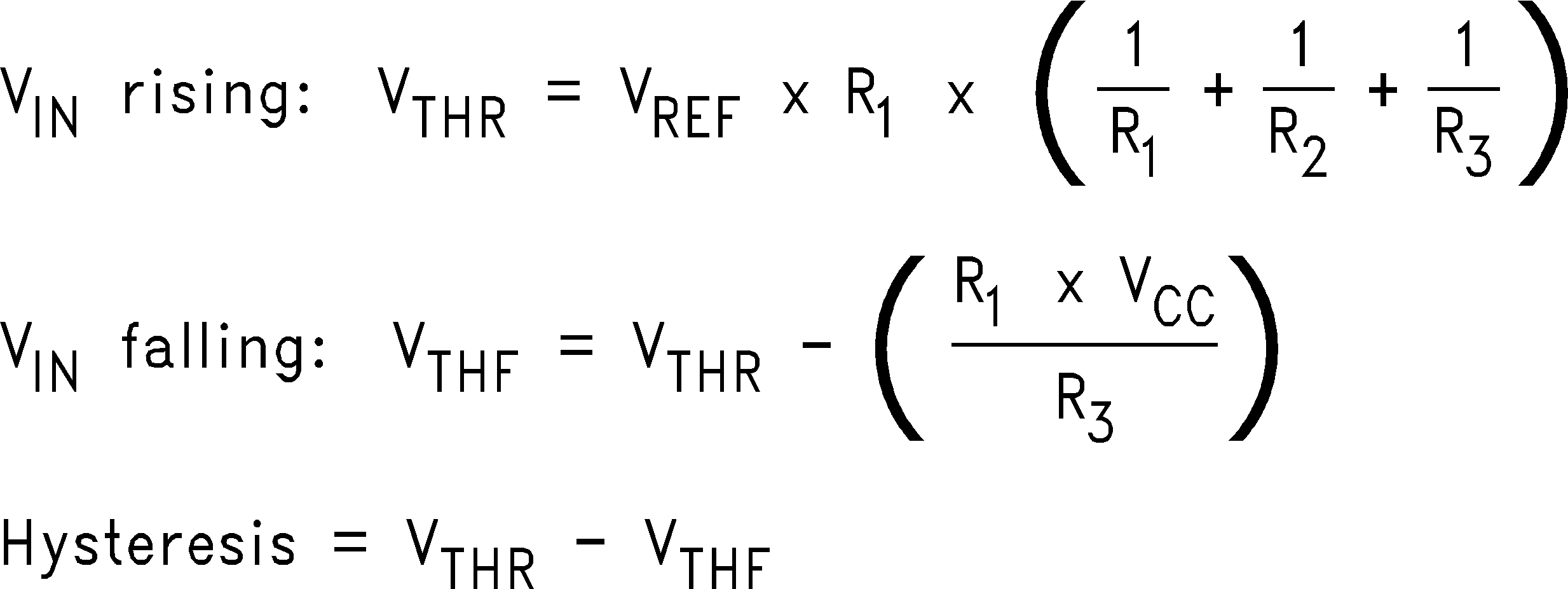
This method is recommended for additional hysteresis of up to a few hundred millivolts. Beyond that, the impedance of R3 is low enough to affect the bias string and adjustment of R1 may be also required.
8.2.2.2 Zero-Crossing Detector
The inverting input is connected to ground and the non-inverting input is connected to 100mVp-p signal. As the signal at the non-inverting input crosses 0 V, the comparator's output Changes State.
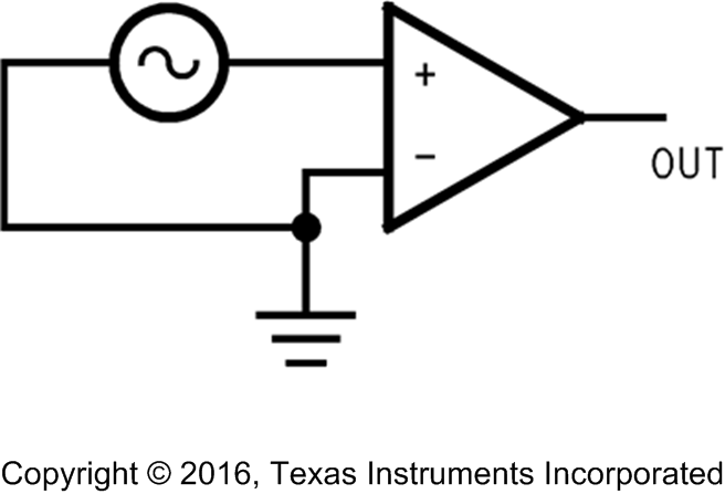 Figure 15. Zero-Crossing Detector
8.2.2.3 Threshold Detector
Instead of tying the inverting input to 0 V, the inverting input can be tied to a reference voltage. The non-inverting input is connected to the input. As the input passes the VREF threshold, the comparator's output changes state.
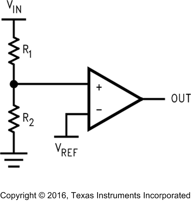 Figure 16. Threshold Detector
8.2.2.4 Crystal Oscillator
A simple crystal oscillator using the LMV7219 is shown in Figure 17. Resistors R1 and R2 set the bias point at the comparator's non-inverting input. Resistors R3, R4 and C1 sets the inverting input node at an appropriate DC average level based on the output. The crystal's path provides resonant positive feedback and stable oscillation occurs. The output duty cycle for this circuit is roughly 50%, but it is affected by resistor tolerances and to a lesser extent by the comparator offset.
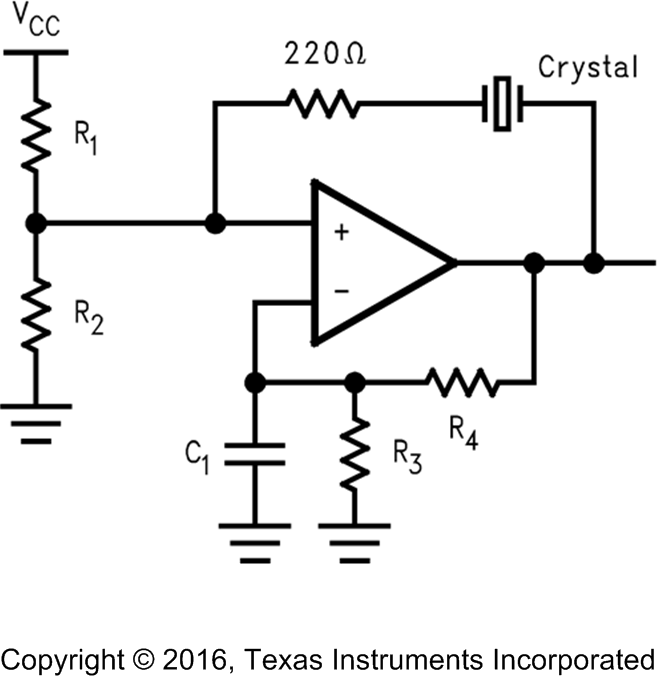 Figure 17. Crystal Oscillator
8.2.2.5 IR Receiver
The LMV7219 is an ideal candidate to be used as an infrared receiver. The infrared photo diode creates a current relative to the amount of infrared light present. The current creates a voltage across RD. When this voltage level cross the voltage applied by the voltage divider to the inverting input, the output transitions.
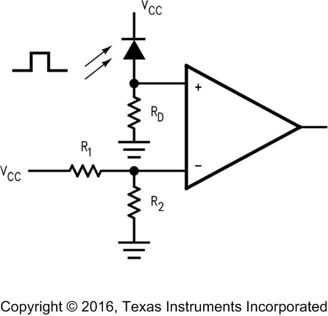 Figure 18. IR Receiver
8.2.3 Application Curve
