ZHCSI25 April 2018 LMV7239-Q1
PRODUCTION DATA.
7.4.4.1 Zero Crossing Detector With Hysteresis
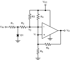
To improve switching times and centering the input threshold to ground a small amount of positive feedback is added to the circuit. Voltage divider R4 and R5 establishes a reference voltage, V1, at the positive input. By making the series resistance, R1 plus R2 equal to R5, the switching condition, V1 = V2, will be satisfied when VIN = 0.
The positive feedback resistor, R6, is made very large with respect to R5 || R6 = 2000 R5). The resultant hysteresis established by this network is very small (ΔV1< 10 mV) but it is sufficient to insure rapid output voltage transitions.
Diode D1 is used to ensure that the inverting input terminal of the comparator never goes below approximately −100 mV. As the input terminal goes negative, D1 will forward bias, clamping the node between R1 and R2 to approximately −700 mV. This sets up a voltage divider with R2 and R3 preventing V2 from going below ground. The maximum negative input overdrive is limited by the current handling ability of D1.
 Figure 22. Zero Crossing Detector With Hysteresis