ZHCSI24O September   2000  – April 2018 LMV7235 , LMV7239

PRODUCTION DATA.  

  1. 特性
  2. 应用
  3. 说明
    1.     Device Images
      1.      电源电流与电源电压间的关系
      2.      传播延迟与过驱动
  4. 修订历史记录
  5. Pin Configuration and Functions
    1.     Pin Functions
  6. Specifications
    1. 6.1 Absolute Maximum Ratings
    2. 6.2 ESD Ratings
    3. 6.3 Recommended Operating Conditions
    4. 6.4 Thermal Information
    5. 6.5 Electrical Characteristics, 2.7 V
    6. 6.6 Electrical Characteristics, 5 V
    7. 6.7 Typical Characteristics
  7. Detailed Description
    1. 7.1 Overview
    2. 7.2 Functional Block Diagram
    3. 7.3 Feature Description
      1. 7.3.1 Input Stage
      2. 7.3.2 Output Stage: LMV7239
      3. 7.3.3 Output Stage: LMV7235
    4. 7.4 Device Functional Modes
      1. 7.4.1 Capacitive and Resistive Loads
      2. 7.4.2 Noise
      3. 7.4.3 Hysteresis
        1. 7.4.3.1 Inverting Comparator With Hysteresis
        2. 7.4.3.2 Non-Inverting Comparator With Hysteresis
      4. 7.4.4 Zero Crossing Detector
        1. 7.4.4.1 Zero Crossing Detector With Hysteresis
      5. 7.4.5 Threshold Detector
  8. Application and Implementation
    1. 8.1 Application Information
    2. 8.2 Typical Applications
      1. 8.2.1 Square Wave Oscillator
        1. 8.2.1.1 Design Requirements
        2. 8.2.1.2 Detailed Design Procedure
        3. 8.2.1.3 Application Curves
      2. 8.2.2 Crystal Oscillator
      3. 8.2.3 Infrared (IR) Receiver
      4. 8.2.4 Window Detector
  9. Power Supply Recommendations
  10. 10Layout
    1. 10.1 Layout Guidelines
    2. 10.2 Layout Example
  11. 11器件和文档支持
    1. 11.1 器件支持
      1. 11.1.1 开发支持
    2. 11.2 文档支持
      1. 11.2.1 相关文档
    3. 11.3 相关链接
    4. 11.4 接收文档更新通知
    5. 11.5 社区资源
    6. 11.6 商标
    7. 11.7 静电放电警告
    8. 11.8 术语表
  12. 12机械、封装和可订购信息

封装选项

机械数据 (封装 | 引脚)
散热焊盘机械数据 (封装 | 引脚)
订购信息

Crystal Oscillator

A simple crystal oscillator using the LMV7235 or LMV7239 is shown in Figure 28. Resistors R1 and R2 set the bias point at the comparator’s noninverting input. Resistors, R3 and R4 and capacitor C1 set the inverting input node at an appropriate DC average level based on the output. The crystal’s path provides resonant positive feedback and stable oscillation occurs. The output duty cycle for this circuit is roughly 50%, but it is affected by resistor tolerances and to a lesser extent by the comparator
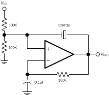
LMV7235 LMV7239 10135902.gifFigure 28. Crystal Oscillator