SNOSA56I February 2003 – September 2015 LMV7271 , LMV7272 , LMV7275
PRODUCTION DATA.
- 1 Features
- 2 Applications
- 3 Description
- 4 Revision History
- 5 Pin Configuration and Functions
-
6 Specifications
- 6.1 Absolute Maximum Ratings
- 6.2 ESD Ratings
- 6.3 Recommended Operating Conditions
- 6.4 Thermal Information
- 6.5 1.8-V Electrical Characteristics
- 6.6 1.8-V AC Electrical Characteristics
- 6.7 2.7-V Electrical Characteristics
- 6.8 2.7-V AC Electrical Characteristics
- 6.9 5-V Electrical Characteristics
- 6.10 5-V AC Electrical Characteristics
- 6.11 Typical Characteristics
-
7 Detailed Description
- 7.1 Overview
- 7.2 Functional Block Diagram
- 7.3 Feature Description
- 7.4 Device Functional Modes
- 8 Application and Implementation
- 9 Power Supply Recommendations
- 10Layout
- 11Device and Documentation Support
- 12Mechanical, Packaging, and Orderable Information
10 Layout
10.1 Layout Guidelines
10.1.1 Circuit Techniques for Avoiding Oscillations in Comparator Applications
Feedback to almost any pin of a comparator can result in oscillation. In addition, when the input signal is a slow voltage ramp or sine wave, the comparator may also burst into oscillation near the crossing point. To avoid oscillation or instability, PCB layout should be engineered thoughtfully. Several precautions are recommended:
- Power supply bypassing is critical, and will improve stability and transient response. Resistance and inductance from power supply wires and board traces increase power supply line impedance. When supply current changes, the power supply line will move due to its impedance. Large enough supply line shift will cause the comparator to mis-operate. To avoid problems, a small bypass capacitor, such as 0.1-µF ceramic, should be placed immediately adjacent to the supply pins. An additional 6.8 μF or greater tantalum capacitor should be placed at the point where the power supply for the comparator is introduced onto the board. These capacitors act as an energy reservoir and keep the supply impedance low. In a dual-supply application, a 0.1-μF capacitor is recommended to be placed across V+ and V− pins.
- Keep all leads short to reduce stray capacitance and lead inductance. It will also minimize any unwanted coupling from any high-level signals (such as the output). The comparators can easily oscillate if the output lead is inadvertently allowed to capacitively couple to the inputs through stray capacitance. This shows up only during the output voltage transition intervals as the comparator changes states. Try to avoid a long loop which could act as an inductor (coil).
- It is a good practice to use an unbroken ground plane on a printed-circuit-board to provide all components with a low inductive ground connection. Make sure ground paths are low-impedance where heavier currents are flowing to avoid ground level shift. Preferably there should be a ground plane under the component.
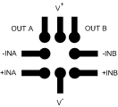
- The output trace should be routed away from inputs. The ground plane should extend between the output and inputs to act as a guard. This can be achieved by running a topside ground plane between the output and inputs. A typical PCB layout is shown in Figure 43.
- When the signal source is applied through a resistive network to one input of the comparator, it is usually advantageous to connect the other input with a resistor with the same value, for both DC and AC consideration. Input traces should be laid out symmetrically if possible.
- All pins of any unused comparators should be tied to the negative supply.
10.1.2 DSBGA Light Sensitivity
Exposing the DSBGA device to direct sunlight will cause mis-operation of the device. Light sources such as Halogen lamps can also affect electrical performance if brought near to the device. The wavelengths, which have the most detrimental effect, are reds and infrareds. Be aware of internal light sources, such as keyboard or display backlights, that may pass through a PCB. A copper plane should be placed on a lower layer under the DSBGA to block light. Be careful using vias under the device, as they may pass light.
10.1.3 DSBGA Mounting
The DSBGA package requires specific mounting techniques, which are detailed in Application Note AN-1112 (SNVA009).
10.1.4 LMV7272 DSBGA to DIP Conversion Board
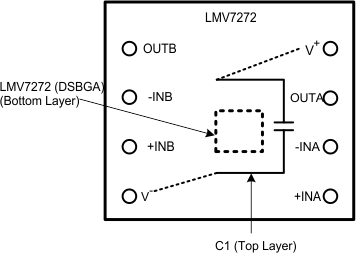
To facilitate characterization and testing, a DSBGA to DIP conversion board, LMV7272TLCONV, is available. It is a 2-layer board, with the LMV7272 mounted on the bottom layer, and a capacitor (C1, between the positive and negative supplies) added to the top layer.
 Figure 42. LMV7272TLCONV Diagram
10.2 Layout Example
 Figure 43. Typical PCB Layout