SNOSA56I February 2003 – September 2015 LMV7271 , LMV7272 , LMV7275
PRODUCTION DATA.
- 1 Features
- 2 Applications
- 3 Description
- 4 Revision History
- 5 Pin Configuration and Functions
-
6 Specifications
- 6.1 Absolute Maximum Ratings
- 6.2 ESD Ratings
- 6.3 Recommended Operating Conditions
- 6.4 Thermal Information
- 6.5 1.8-V Electrical Characteristics
- 6.6 1.8-V AC Electrical Characteristics
- 6.7 2.7-V Electrical Characteristics
- 6.8 2.7-V AC Electrical Characteristics
- 6.9 5-V Electrical Characteristics
- 6.10 5-V AC Electrical Characteristics
- 6.11 Typical Characteristics
-
7 Detailed Description
- 7.1 Overview
- 7.2 Functional Block Diagram
- 7.3 Feature Description
- 7.4 Device Functional Modes
- 8 Application and Implementation
- 9 Power Supply Recommendations
- 10Layout
- 11Device and Documentation Support
- 12Mechanical, Packaging, and Orderable Information
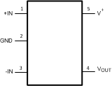
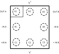
5 Pin Configuration and Functions
DBV or DGK Package
5-Pin SOT-23 or SC70
Top View

YZR Package
8-Pin DSBGA
Top View

See DSBGA Light Sensitivity and DSBGA Mounting in the Layout Guidelines section for mounting precautions.
Pin Functions
| PIN | I/O | DESCRIPTION | ||
|---|---|---|---|---|
| NAME | SOT-23, SC70 | DSBGA | ||
| +IN | 1 | — | I | Noninverting Input |
| GND | 2 | — | P | Negative Supply Voltage |
| -IN | 3 | — | I | Invering Input |
| VOUT | 4 | — | O | Output |
| V+ | 5 | A2 | P | Positive Supply Voltage |
| OUT A | — | A1 | O | Output, Channel A |
| -IN A | — | B1 | I | Inverting Input, Channel A |
| +IN A | — | C1 | I | Noninverting Input, Channel A |
| V- | — | C2 | P | Negative Supply Voltage |
| +IN B | — | C3 | I | Noninverting Input, Channel B |
| -IN B | — | B3 | I | Inverting Input, Channel B |
| OUT B | — | A3 | O | Output, Channel B |