ZHCSE55 September 2015 LMV7275-Q1
PRODUCTION DATA.
- 1 特性
- 2 应用
- 3 说明
- 4 修订历史记录
- 5 Pin Configuration and Functions
-
6 Specifications
- 6.1 Absolute Maximum Ratings
- 6.2 ESD Ratings LMV7275-Q1
- 6.3 Recommended Operating Conditions
- 6.4 Thermal Information
- 6.5 1.8-V Electrical Characteristics
- 6.6 1.8-V AC Electrical Characteristics
- 6.7 2.7-V Electrical Characteristics
- 6.8 2.7-V AC Electrical Characteristics
- 6.9 5-V Electrical Characteristics
- 6.10 5-V AC Electrical Characteristics
- 6.11 Typical Characteristics
- 7 Detailed Description
- 8 Application and Implementation
- 9 Power Supply Recommendations
- 10Layout
- 11器件和文档支持
- 12机械、封装和可订购信息
10 Layout
10.1 Layout Guidelines
10.1.1 Circuit Techniques for Avoiding Oscillations in Comparator Applications
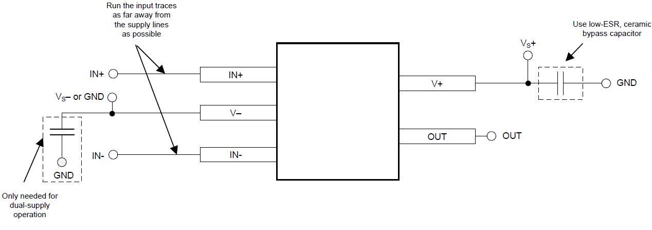
Feedback to almost any pin of a comparator can result in oscillation. In addition, when the input signal is a slow voltage ramp or sine wave, the comparator may also burst into oscillation near the crossing point. To avoid oscillation or instability, PCB layout should be engineered thoughtfully. Several precautions are recommended:
- Power supply bypassing is critical, and will improve stability and response time. Resistance and inductance from power supply wires and board traces increase power supply line impedance. When supply current changes, the power supply line will move due to its impedance. Large enough supply line shift will cause the comparator to malfunction. To avoid problems, a small bypass capacitor, such as 0.1-µF ceramic, should be placed immediately adjacent to the supply pins. An additional 6.8 μF or greater tantalum capacitor should be placed at the point where the power supply for the comparator is introduced onto the board. These capacitors act as an energy reservoir and keep the supply impedance low. In a dual-supply application, a 0.1-μF capacitor is recommended to be placed across V+ and V− pins.
- Keep all leads short to reduce stray capacitance and lead inductance. It will also minimize any unwanted coupling from any high-level signals (such as the output). The comparators can easily oscillate if the output lead is inadvertently allowed to capacitively couple to the inputs through stray capacitance. This shows up only during the output voltage transition intervals as the comparator changes states. Try to avoid a long loop which could act as an inductor (coil).
- It is a good practice to use an unbroken ground plane on a printed-circuit-board to provide all components with a low inductive ground connection. Make sure ground paths are low-impedance where heavier currents are flowing to avoid ground level shift. Preferably there should be a ground plane under the component.
- The output trace should be routed away from inputs. The ground plane should extend between the output and inputs to act as a guard. This can be achieved by running a topside ground plane between the output and inputs. A typical PCB layout is shown in Figure 35.
- When the signal source is applied through a resistive network to one input of the comparator, it is usually advantageous to connect the other input with a resistor with the same value, for both DC and AC consideration. Input traces should be laid out symmetrically if possible.
10.2 Layout Example
 Figure 35. Typical PCB Layout