SNOS993P November 2001 – April 2017 LMV931-N , LMV932-N , LMV934-N
PRODUCTION DATA.
- 1 Features
- 2 Applications
- 3 Description
- 4 Revision History
- 5 Pin Configuration and Functions
-
6 Specifications
- 6.1 Absolute Maximum Ratings
- 6.2 ESD Ratings (Commercial)
- 6.3 Recommended Operating Ratings
- 6.4 Thermal Information
- 6.5 DC Electrical Characteristics 1.8 V
- 6.6 AC Electrical Characteristics 1.8 V
- 6.7 DC Electrical Characteristics 2.7 V
- 6.8 AC Electrical Characteristics 2.7 V
- 6.9 Electrical Characteristics 5 V DC
- 6.10 AC Electrical Characteristics 5 V
- 6.11 Typical Characteristics
- 7 Detailed Description
- 8 Application and Implementation
- 9 Power Supply Recommendations
- 10Layout
- 11Device and Documentation Support
- 12Mechanical, Packaging, and Orderable Information
5 Pin Configuration and Functions
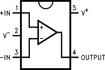
DBV and DCK Package
5-Pin SC-70 and SOT-23
LMV931-N Top View

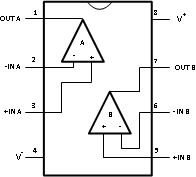
DGK and D Package
8-Pin VSSOP and SOIC
LMV932-N Top View

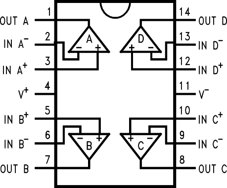
DGK and D Package
14-Pin TSSOP and SOIC
LMV934-N Top View

Pin Functions: LMV931
| PIN | I/O | DESCRIPTION | |||
|---|---|---|---|---|---|
| NAME | LMV931 DBV, DCK | ||||
| +IN | 1 | I | Noninverting Input | ||
| -IN | 3 | I | Inverting Input | ||
| OUT | 4 | O | Output | ||
| V- | 2 | P | Negative Supply | ||
| V+ | 5 | P | Positive Supply | ||
Pin Functions: LMV932 and LMV934
| PIN | I/O | DESCRIPTION | |||
|---|---|---|---|---|---|
| NAME | LMV932 D, DGK | LMV934 D, PW | |||
| +IN A | 3 | 3 | I | Noninverting input, channel A | |
| +IN B | 5 | 5 | I | Noninverting input, channel B | |
| +IN C | — | 10 | I | Noninverting input, channel C | |
| +IN D | — | 12 | I | Noninverting input, channel D | |
| –IN A | 2 | 2 | I | Inverting input, channel A | |
| –IN B | 6 | 6 | I | Inverting input, channel B | |
| –IN C | — | 9 | I | Inverting input, channel C | |
| –IN D | — | 13 | I | Inverting input, channel D | |
| OUT A | 1 | 1 | O | Output, channel A | |
| OUT B | 7 | 7 | O | Output, channel B | |
| OUT C | — | 8 | O | Output, channel C | |
| OUT D | — | 14 | O | Output, channel D | |
| V+ | 8 | 4 | P | Positive (highest) power supply | |
| V– | 4 | 11 | P | Negative (lowest) power supply | |