SNAS187D February 2003 – January 2016 LMX2430 , LMX2433 , LMX2434
PRODUCTION DATA.
- 1 Features
- 2 Applications
- 3 Description
- 4 Revision History
- 5 Description continued
- 6 Pin Configuration and Functions
- 7 Specifications
- 8 Parameter Measurement Information
-
9 Detailed Description
- 9.1 Overview
- 9.2 Functional Block Diagram
- 9.3 Feature Description
- 9.4 Device Functional Modes
- 9.5 Programming
- 9.6
Register Maps
- 9.6.1 Control Register Content Map
- 9.6.2
R0 Register
- 9.6.2.1 RF_R[14:0] - RF Synthesizer Programmable Reference Divider (R Counter) (R0[17:3])
- 9.6.2.2 RF_CPP - RF Synthesizer Phase Detector Polarity (R0[18])
- 9.6.2.3 RF_CPG - RF Synthesizer Charge-Pump Current Gain (R0[19])
- 9.6.2.4 RF_CPT - RF Synthesizer Charge-Pump Tri-State (R0[20])
- 9.6.2.5 RF_RST - RF Synthesizer Counter Reset (R0[21])
- 9.6.3 R1 Register
- 9.6.4
R2 Register
- 9.6.4.1 RF_TOC[0:11] - RF Synthesizer Time-Out Counter (R2[14:3])
- 9.6.4.2
R3 Register
- 9.6.4.2.1 IF_R[14:0] - IF Synthesizer Programmable Reference Divider (R Counter) (R3[17:3])
- 9.6.4.2.2 IF_CPP - IF Synthesizer Phase Detector Polarity (R3[18])
- 9.6.4.2.3 IF_CPG - IF Synthesizer Charge-Pump Current Gain (R3[19])
- 9.6.4.2.4 IF_CPT - IF Synthesizer Charge-Pump Tri-State (R3[20])
- 9.6.4.2.5 IF_RST - IF Synthesizer Counter Reset (R3[21])
- 9.6.5 R4 Register
- 9.6.6 R5 Register
- 9.6.7 MUX[3:0] - Multifunction Output Select (R3[23:22]:R0[23:22])
- 10Application and Implementation
- 11Power Supply Recommendations
- 12Layout
- 13Device and Documentation Support
- 14Mechanical, Packaging, and Orderable Information
10 Application and Implementation
NOTE
Information in the following applications sections is not part of the TI component specification, and TI does not warrant its accuracy or completeness. TI’s customers are responsible for determining suitability of components for their purposes. Customers should validate and test their design implementation to confirm system functionality.
10.1 Application Information
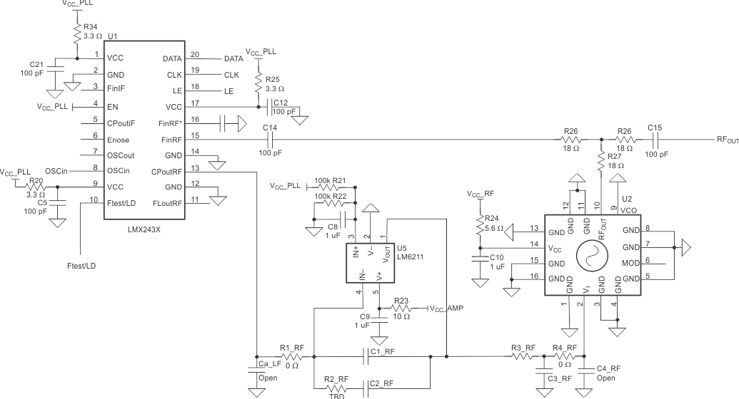
The LMX2430 family of devices can be used in a broad class of applications. LMX2430x devices have very low current consumption and are well-suited for many lower power applications. Because these devices have two PLLs, they can be used to generate two distinct frequencies. However, it is a perfectly valid thing to only use one of the PLLs and power down the other side. When only one side is used, be sure to power the other side down, but do NOT disconnect the power pins for the unused side as they are shared across several internal blocks. When the unused side is powered down, it draws no current, and the counters and charge pump are not running or generating any noise and spurs. Figure 33 generally applies to most applications.
10.2 Typical Application
 Figure 33. Typical Use Case
10.2.1 Design Requirements
Table 41 lists the design parameters of the LMX243x.
Table 41. Design Parameters
| PARAMETER | VALUE | |
|---|---|---|
| KPD | Charge-Pump Gain | 4 mA |
| CVCO | VCO Input Capacitance | 22 pF |
| fPD | Phase Detector Frequency | 1 MHz |
| fOSC | OSCin Frequency | 100 MHz |
| BW | Loop Bandwidth | 31.1 kHz |
| PM | Phase Margin | 59.6 degrees |
| Gamma | Gamma | 0.9 |
| T3/T1 | T3/T1 Ratio | 177.1% |
| C1_RF | Loop Filter Components | 270 pF |
| C2_RF | 10 nF | |
| C3_RF | 1 nF | |
| C4_RF | Open | |
| R2_RF | 1.8 Ω | |
| R3_RF | 820 Ω | |
| R4_RF | 0 Ω | |
10.2.2 Detailed Design Procedure
The loop filter design is key and involves trade-offs between lock time, phase noise, and spurs. The TI website has references and design and simulation tools that can be used to design the loop filter and simulate the performance.
10.2.3 Application Curves
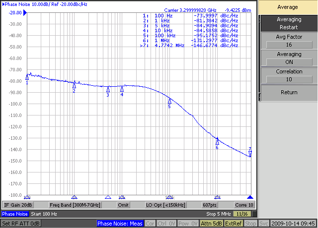
 Figure 34. Phase Noise
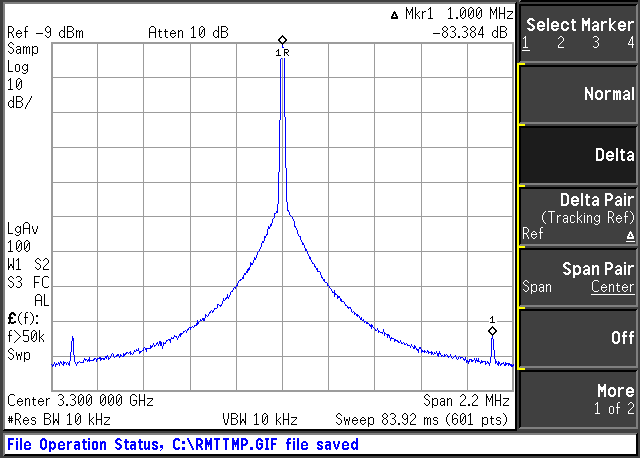
 Figure 35. Phase Detector Spurs