SNAS187D February 2003 – January 2016 LMX2430 , LMX2433 , LMX2434
PRODUCTION DATA.
- 1 Features
- 2 Applications
- 3 Description
- 4 Revision History
- 5 Description continued
- 6 Pin Configuration and Functions
- 7 Specifications
- 8 Parameter Measurement Information
-
9 Detailed Description
- 9.1 Overview
- 9.2 Functional Block Diagram
- 9.3 Feature Description
- 9.4 Device Functional Modes
- 9.5 Programming
- 9.6
Register Maps
- 9.6.1 Control Register Content Map
- 9.6.2
R0 Register
- 9.6.2.1 RF_R[14:0] - RF Synthesizer Programmable Reference Divider (R Counter) (R0[17:3])
- 9.6.2.2 RF_CPP - RF Synthesizer Phase Detector Polarity (R0[18])
- 9.6.2.3 RF_CPG - RF Synthesizer Charge-Pump Current Gain (R0[19])
- 9.6.2.4 RF_CPT - RF Synthesizer Charge-Pump Tri-State (R0[20])
- 9.6.2.5 RF_RST - RF Synthesizer Counter Reset (R0[21])
- 9.6.3 R1 Register
- 9.6.4
R2 Register
- 9.6.4.1 RF_TOC[0:11] - RF Synthesizer Time-Out Counter (R2[14:3])
- 9.6.4.2
R3 Register
- 9.6.4.2.1 IF_R[14:0] - IF Synthesizer Programmable Reference Divider (R Counter) (R3[17:3])
- 9.6.4.2.2 IF_CPP - IF Synthesizer Phase Detector Polarity (R3[18])
- 9.6.4.2.3 IF_CPG - IF Synthesizer Charge-Pump Current Gain (R3[19])
- 9.6.4.2.4 IF_CPT - IF Synthesizer Charge-Pump Tri-State (R3[20])
- 9.6.4.2.5 IF_RST - IF Synthesizer Counter Reset (R3[21])
- 9.6.5 R4 Register
- 9.6.6 R5 Register
- 9.6.7 MUX[3:0] - Multifunction Output Select (R3[23:22]:R0[23:22])
- 10Application and Implementation
- 11Power Supply Recommendations
- 12Layout
- 13Device and Documentation Support
- 14Mechanical, Packaging, and Orderable Information
7 Specifications
7.1 Absolute Maximum Ratings
See (1)(2)(3)(4)| MIN | MAX | UNIT | ||
|---|---|---|---|---|
| Power supply voltage VCC to GND |
−0.3 | 3.25 | V | |
| VI | Voltage on any pin to GND VI must be < +3.25 V |
−0.3 | VCC + 0.3 | V |
| TL | Lead temperature (solder 4 seconds) | 260 | °C | |
| Tstg | Storage temperature | −65 | 150 | °C |
(1) Stresses beyond those listed under Absolute Maximum Ratings may cause permanent damage to the device. These are stress ratings only, which do not imply functional operation of the device at these or any other conditions beyond those indicated under Recommended Operating Conditions. Exposure to absolute-maximum-rated conditions for extended periods may affect device reliability.
(2) This device is a high-performance RF integrated circuit with an ESD rating < 2000 V and is ESD-sensitive. Handling and assembly of this device must be done at ESD-protected work stations.
(3) GND = 0 V.
(4) If Military/Aerospace specified devices are required, contact the Texas Instruments Sales Office/Distributors for availability and specifications.
7.2 Recommended Operating Conditions
| MIN | MAX | UNIT | |
|---|---|---|---|
| Power supply voltage Vcc to GND | 2.25 | 2.75 | V |
| Operating temperature, TA | −40 | 85 | °C |
7.3 Thermal Information
| THERMAL METRIC(1) | LMX243x | UNIT | ||
|---|---|---|---|---|
| NPE (ULGA) | PW (TSSOP) | |||
| 20 PINS | 20 PINS | |||
| RθJA | Junction-to-ambient thermal resistance | 80.9 | 111.5 | °C/W |
| RθJC(top) | Junction-to-case (top) thermal resistance | 22.5 | 44.9 | °C/W |
| RθJB | Junction-to-board thermal resistance | 40 | 63.5 | °C/W |
| ψJT | Junction-to-top characterization parameter | 0.2 | 6.1 | °C/W |
| ψJB | Junction-to-board characterization parameter | 40 | 62.8 | °C/W |
(1) For more information about traditional and new thermal metrics, see the Semiconductor and IC Package Thermal Metrics application report, SPRA953.
7.4 Electrical Characteristics
VCC = EN = 2.5 V, −40°C ≤ TA ≤ +85°C, unless otherwise specified| PARAMETER | TEST CONDITIONS | MIN | TYP | MAX | UNIT | ||
|---|---|---|---|---|---|---|---|
| ICC PARAMETERS | |||||||
| ICCRF | Power supply current, RF synthesizer |
LMX2430 | CLK, DATA and LE = 0 V OSCin = GND RF_PD Bit = 0 IF_PD Bit = 1 RF_P Bit = 0 |
2.8 | 3.6 | mA | |
| LMX2433 | 3.2 | 4.4 | mA | ||||
| LMX2434 | 4.6 | 6.2 | mA | ||||
| ICCIF | Power supply current, IF synthesizer |
LMX2430 | CLK, DATA and LE = 0 V OSCin = GND RF_PD Bit = 1 IF_PD Bit = 0 IF_P Bit = 0 |
1.4 | 2 | mA | |
| LMX2433 | 2 | 2.8 | mA | ||||
| LMX2434 | 2.4 | 3.5 | mA | ||||
| ICCPD | Power-down current | EN, ENosc, CLK, DATA and LE = 0 V |
10 | μA | |||
| RF SYNTHESIZER PARAMETERS | |||||||
| fFinRF | RF operating frequency |
LMX2430 | RF_P Bit = 0 | 250 | 2500 | MHz | |
| RF_P Bit = 1 | 250 | 3000 | MHz | ||||
| LMX2433 | RF_P Bit = 0 | 500 | 3000 | MHz | |||
| RF_P Bit = 1 | 500 | 3600 | MHz | ||||
| LMX2434 | RF_P Bit = 0 or 1 | 1000 | 5000 | MHz | |||
| NRF | N divider range | P = 8 / 9(1) | 24 | 262,151 | |||
| P = 16 / 17(1) | 48 | 524,287 | |||||
| P = 32 / 33(1) | 96 | 524,287 | |||||
| RRF | RF R divider range | 3 | 32,767 | ||||
| fCOMPRF | RF phase detector frequency | 10 | MHz | ||||
| pFinRF | RF input sensitivity | LMX2430 / 33 2.25 V ≤ VCC ≤ 2.75 V(2) |
−15 | 0 | dBm | ||
| LMX2434 2.35 V ≤ VCC ≤ 2.75 V(2) |
−12 | 0 | dBm | ||||
| ICPoutRF
Source |
RF charge-pump output source current | VCPoutRF = VCC / 2 RF_CPG Bit = 0(3) |
–1 | mA | |||
| VCPoutRF = VCC / 2 RF_CPG Bit = 1(3) |
–4 | mA | |||||
| ICPoutRF
Sink |
RF charge-pump output sink current | VCPoutRF = VCC / 2 RF_CPG Bit = 0(3) |
1 | mA | |||
| VCPoutRF = VCC / 2 RF_CPG Bit = 1(3) |
4 | mA | |||||
| ICPoutRF
TRI |
RF charge-pump output tri-state current | 0.5 V ≤ VCPoutRF ≤ VCC – 0.5 V(3) | –2.5 | 2.5 | nA | ||
| ICPoutRF
%MIS |
RF charge-pump output sink current vs charge-pump output source current mismatch | VCPoutRF = VCC / 2(4) | 3% | 10% | |||
| ICPoutRF
%VCPoutRF |
RF charge-pump output current magnitude variation vs charge-pump output voltage | 0.5 V ≤ VCPoutRF ≤ VCC – 0.5 V(4) | 5% | 15% | |||
| ICPoutRF
%TA |
RF charge-pump output current magnitude variation vs temperature | VCPoutRF = VCC / 2(4) | 2% | ||||
| IF SYNTHESIZER PARAMETERS | |||||||
| fFinIF | IF operating frequency | LMX2430 | IF_P Bit = 0 or 1 | 100 | 800 | MHz | |
| LMX2433 | IF_P Bit = 0 or 1 | 250 | 1700 | MHz | |||
| LMX2434 | IF_P Bit = 0 or 1 | 500 | 2500 | MHz | |||
| NIF | IF N divider range | P = 8/9(1) | 24 | 131,079 | |||
| P = 16/17(1) | 48 | 262,143 | |||||
| RIF | IF R divider range | 3 | 32,767 | ||||
| fCOMPIF | IF phase detector frequency | 10 | MHz | ||||
| pFinIF | IF input sensitivity | 2.25 V ≤ VCC ≤ 2.75 V(2) | –15 | 0 | dBm | ||
| ICPoutIF
Source |
IF charge-pump output source current | VCPoutIF = VCC/2 IF_CPG Bit = 0(3) |
–1 | mA | |||
| VCPoutIF = VCC/2 IF_CPG Bit = 1(3) |
–4 | mA | |||||
| ICPoutIF
Sink |
IF charge-pump output sink current | VCPoutIF = VCC/2 IF_CPG Bit = 0(3) |
1 | mA | |||
| VCPoutIF = VCC/2 IF_CPG Bit = 1(3) |
4 | mA | |||||
| ICPoutIF
TRI |
IF charge-pump output tri-state current | 0.5 V ≤ VCPoutIF ≤ VCC – 0.5 V(3) | –2.5 | 2.5 | nA | ||
| ICPoutIF
%MIS |
IF charge-pump output sink current vs charge-pump output source current mismatch | VCPoutIF = VCC/2(4) | 3% | 10% | |||
| ICPoutIF
%VCPoutIF |
IF charge-pump output current magnitude variation vs charge-pump output voltage | 0.5 V ≤ VCPoutIF ≤ VCC – 0.5 V(4) | 5% | 15% | |||
| ICPoutIF
%TA |
IF charge-pump output current magnitude variation vs temperature | VCPoutIF = VCC/2(4) | 2% | ||||
| OSCILLATOR PARAMETERS | |||||||
| fOSCin | Oscillator operating frequency | 1 | 256 | MHz | |||
| vOSCin | Oscillator sensitivity | See (5) | 0.5 | VCC | VPP | ||
| IOSCin | Oscillator input current | VOSCin = VCC | 100 | µA | |||
| VOSCin = 0 V | –100 | µA | |||||
| DIGITAL INTERFACE (DATA, CLK, LE, EN, ENosc, Ftest/LD, FLoutRF, OSCout/ FLoutIF) | |||||||
| VIH | High-level input voltage | 1.6 | V | ||||
| VIL | Low-level input voltage | 0.4 | V | ||||
| IIH | High-level input current | VIH = VCC | 1 | μA | |||
| IIL | Low-level input current | VIL = 0 V | −1 | μA | |||
| VOH | High-level output voltage | IOH = −500 μA | VCC − 0.4 | V | |||
| VOL | Low-level output voltage | IOL = 500 μA | 0.4 | V | |||
| PHASE NOISE CHARACTERISTICS | |||||||
| LNRF(f) | RF synthesizer normalized phase noise contribution(7) | TCXO Reference Source RF_CPG Bit = 1 IF_PD Bit = 1 |
–219 | dBc/ Hz | |||
| LNIF(f) | IF synthesizer normalized phase noise contribution(7) | TCXO Reference Source IF_CPG Bit = 1 RF_PD Bit = 1 |
–214 | dBc/ Hz | |||
| LRF(f) | RF synthesizer single-side band phase noise measured | LMX2430 | fFinRF = 2750 MHz f = 10-kHz offset fCOMPRF = 1 MHz Loop Bandwidth = 100 kHz NRF = 2750 fOSCin = 10 MHz vOSCin = 1 VPP RF_CPG Bit = 1 IF_PD Bit = 1 TA = 25oC(8) |
–90.3 | dBc/ Hz | ||
| LMX2433 | fFinRF = 3200 MHz f = 10-kHz offset fCOMPRF = 1 MHz Loop Bandwidth = 100 kHz NRF = 3200 fOSCin = 10 MHz vOSCin = 1 VPP RF_CPG Bit = 1 IF_PD Bit = 1 TA = 25°C(8) |
–88.9 | dBc/ Hz | ||||
| LMX2434 | fFinRF = 4700 MHz f = 10-kHz offset fCOMPRF = 1 MHz Loop Bandwidth = 100 kHz NRF = 4700 fOSCin = 10 MHz vOSCin = 1 VPP RF_CPG Bit = 1 IF_PD Bit = 1 TA = 25°C(8) |
–85.6 | dBc/ Hz | ||||
(1) Some of the values in this range are illegal divide ratios (B < A). To obtain continuous legal division, the Minimum Divide Ratio must be calculated. Use N ≥ P * (P−1), where P is the value of the prescaler selected.
(2) Refer to LMX243x FinRF Sensitivity Test Set-Up.
(3) Refer to LMX243x Charge Pump Test Set-Up.
(4) Refer to Charge Pump Current Specification Definitions for details on how these measurements are made.
(5) Refer to LMX243x OSCin Sensitivity Test Set-Up.
(6) Refer to LMX243x Serial Data Input Timing figure.
(7) Normalized Phase Noise Contribution is defined as LN(f) = L(f) − 20 log (N) − 10 log (fCOMP), where L(f) is defined as the single side band phase noise measured at an offset frequency, f, in a 1-Hz bandwidth. The offset frequency, f, must be chosen sufficiently smaller than the loop bandwidth of the PLL, yet large enough to avoid substantial phase noise contribution from the reference source. N is the value selected for the feedback divider and fCOMP is the RF/IF phase and frequency detector comparison frequency.
(8) The synthesizer phase noise is measured with the LMX2430PW/LMX2430NPE evaluation boards and the HP8566B Spectrum Analyzer.
7.5 Timing Requirements
See (6)| MIN | NOM | MAX | UNIT | |||
|---|---|---|---|---|---|---|
| MICROWIRE INTERFACE | ||||||
| tCS | DATA to CLK set-up time | 50 | ns | |||
| tCH | DATA to CLK hold time | 10 | ns | |||
| tCWH | CLK pulse width HIGH | 50 | ns | |||
| tCWL | CLK pulse width LOW | 50 | ns | |||
| tES | CLK to LE set-up time | 50 | ns | |||
| tEW | LE pulse width | 50 | ns | |||
7.6 Typical Characteristics
7.6.1 Sensitivity
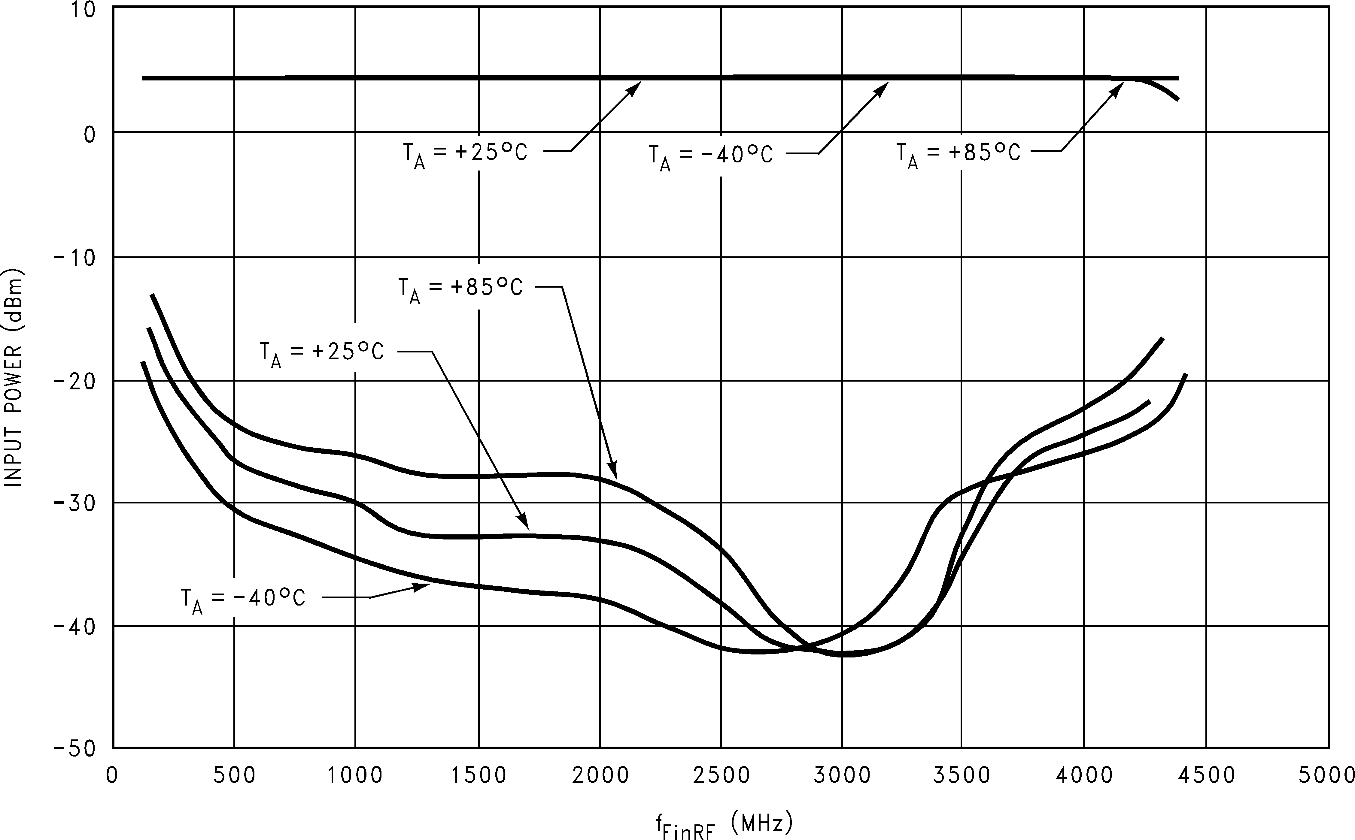
VCC = EN = 2.25 V
Figure 1. LMX2430 FinRF Input Power vs Frequency
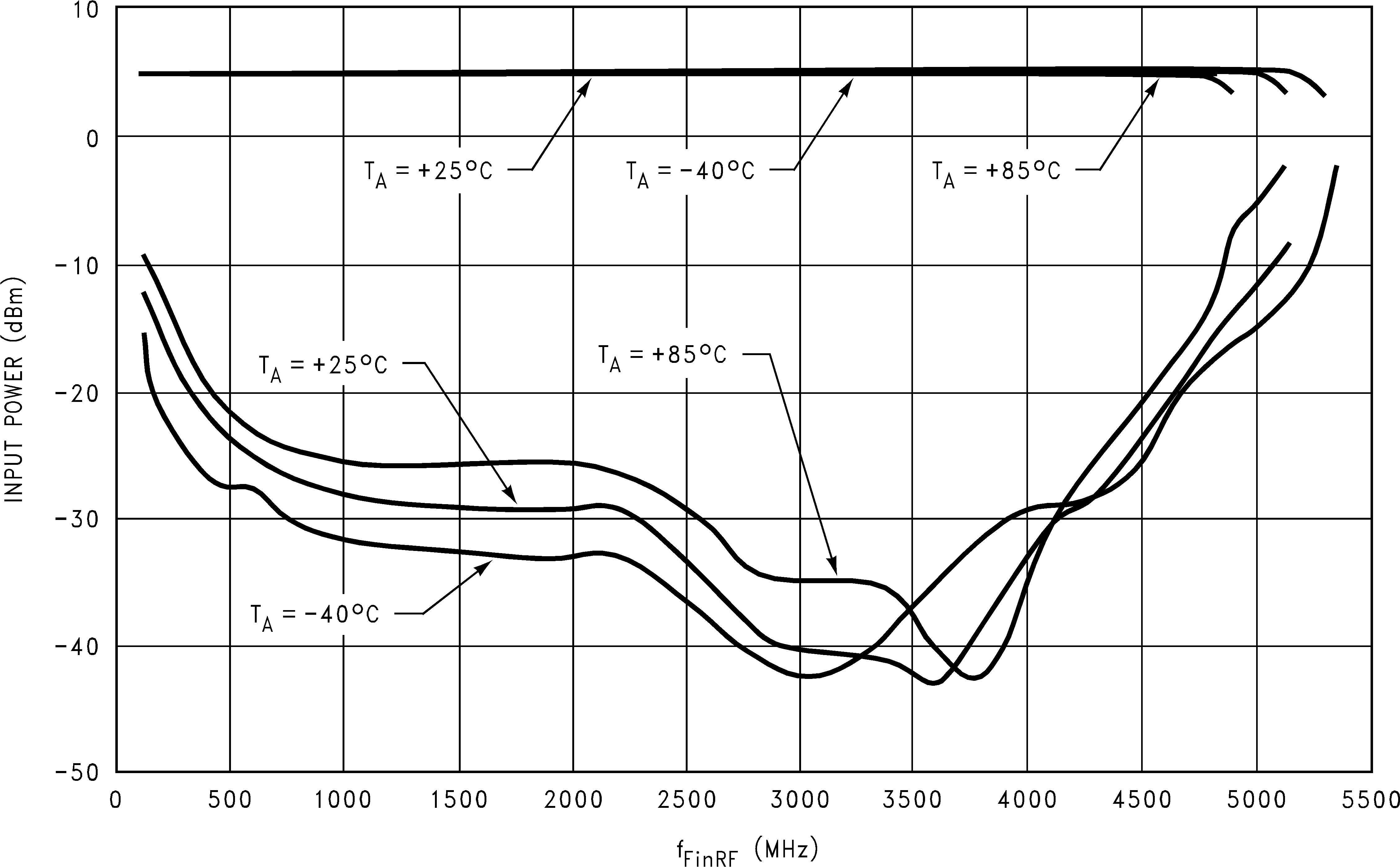
VCC = EN = 2.25 V
Figure 3. LMX2433 FinRF Input Power vs Frequency
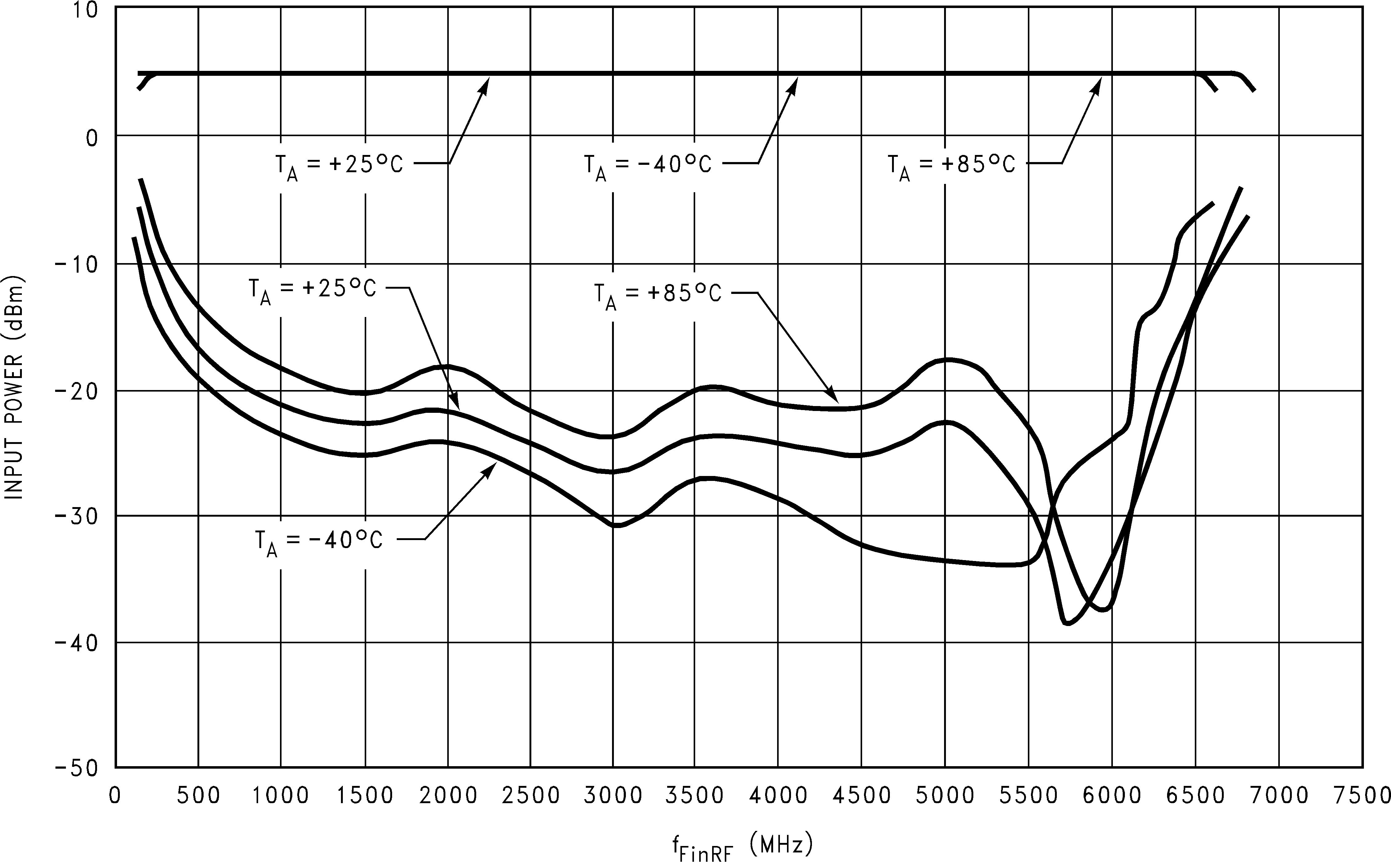
VCC = EN = 2.35 V
Figure 5. LMX2434 FinRF Input Power vs Frequency
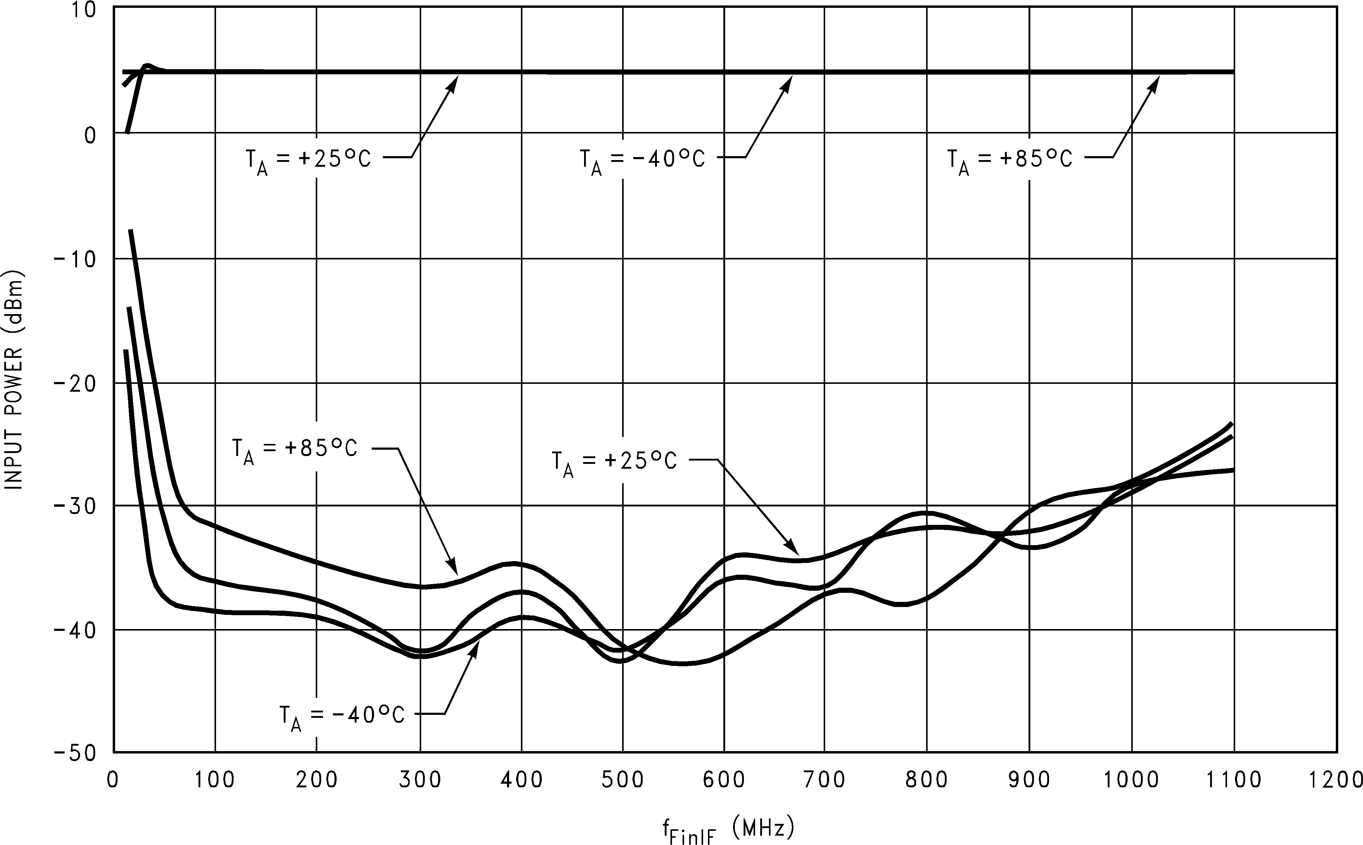
VCC = EN = 2.25 V
Figure 7. LMX2430 FinIF Input Power vs Frequency
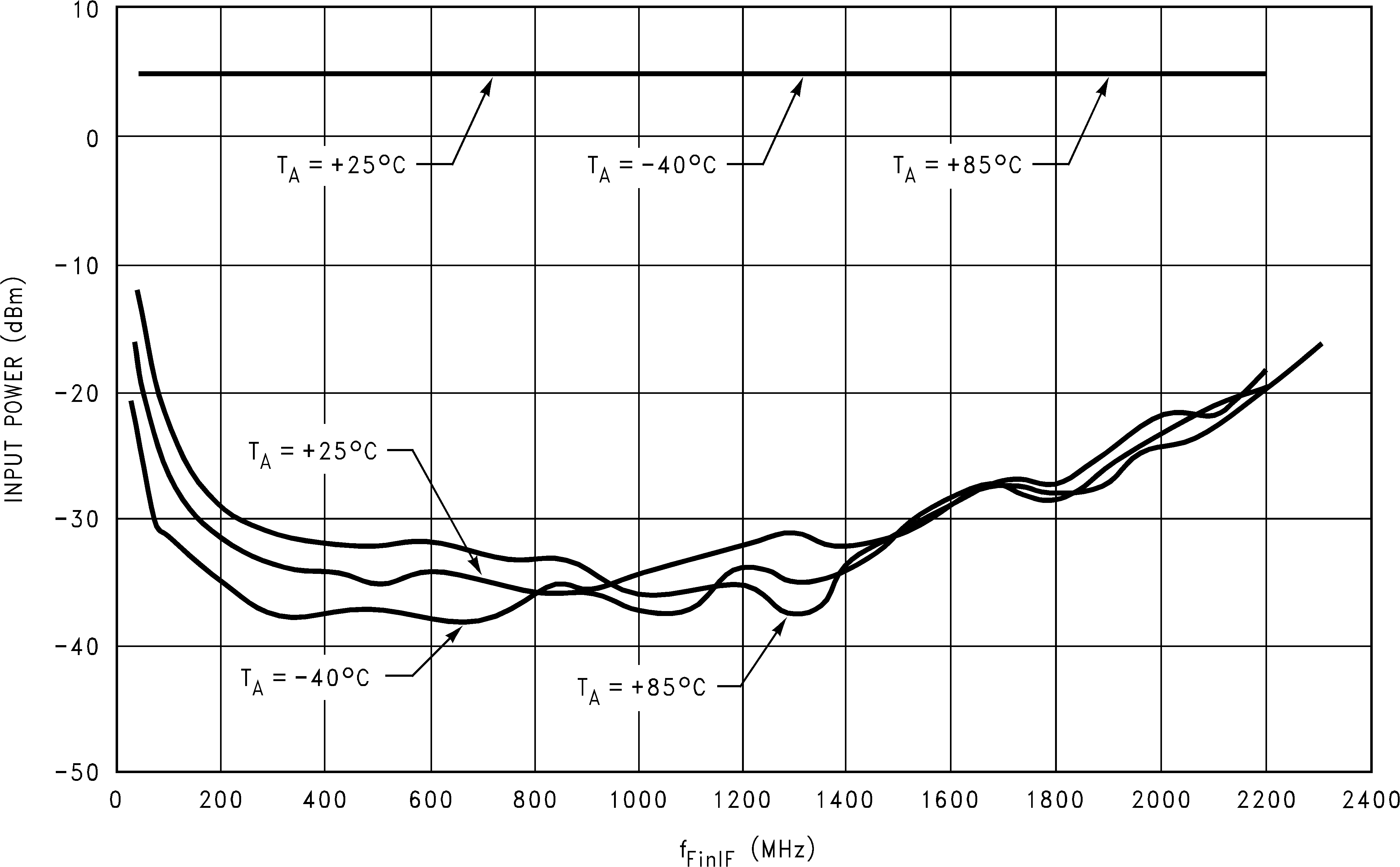
VCC = EN = 2.25 V
Figure 9. LMX2433 FinIF Input Power vs Frequency
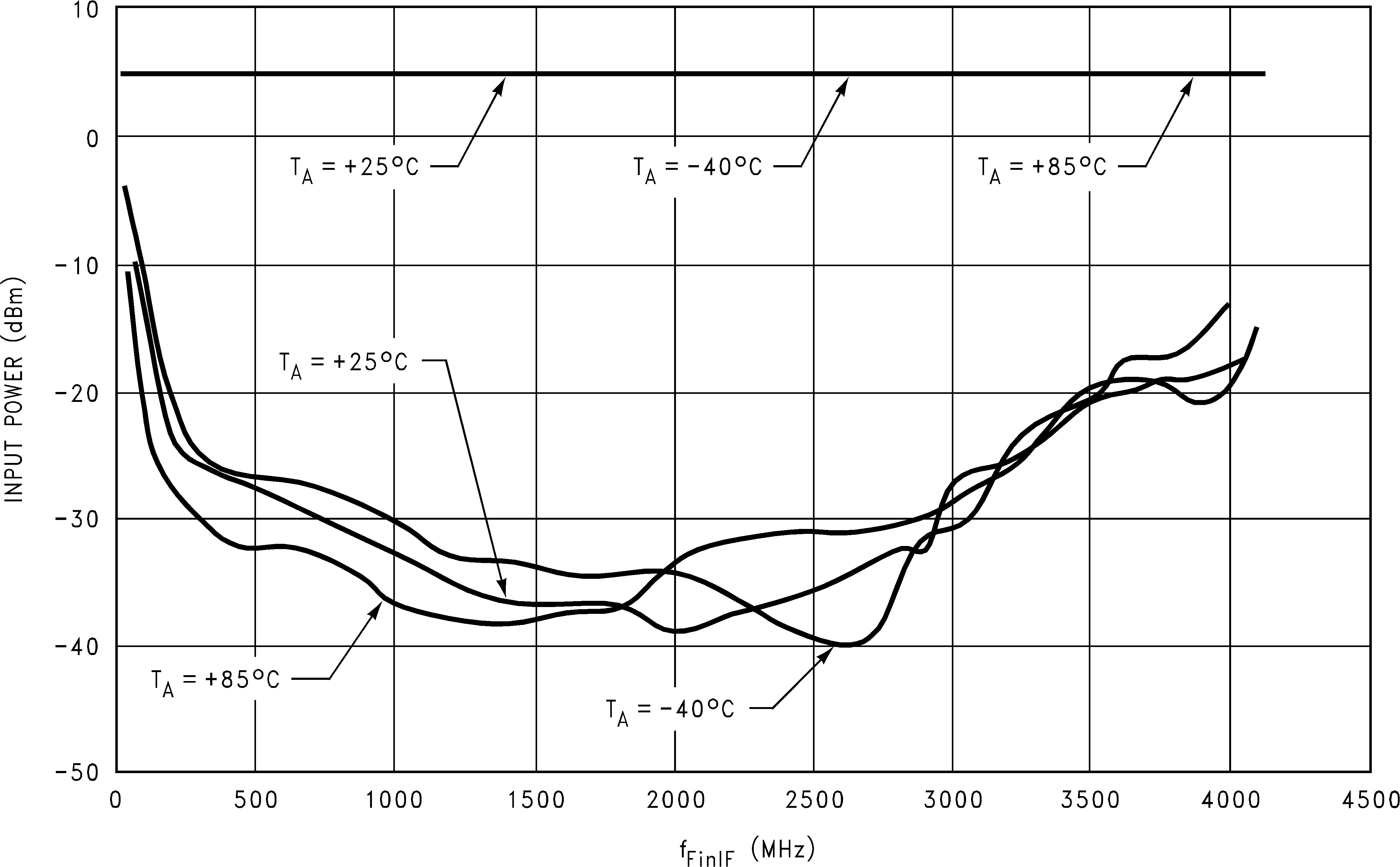
VCC = EN = 2.25 V
Figure 11. LMX2434 FinIF Input Power vs Frequency
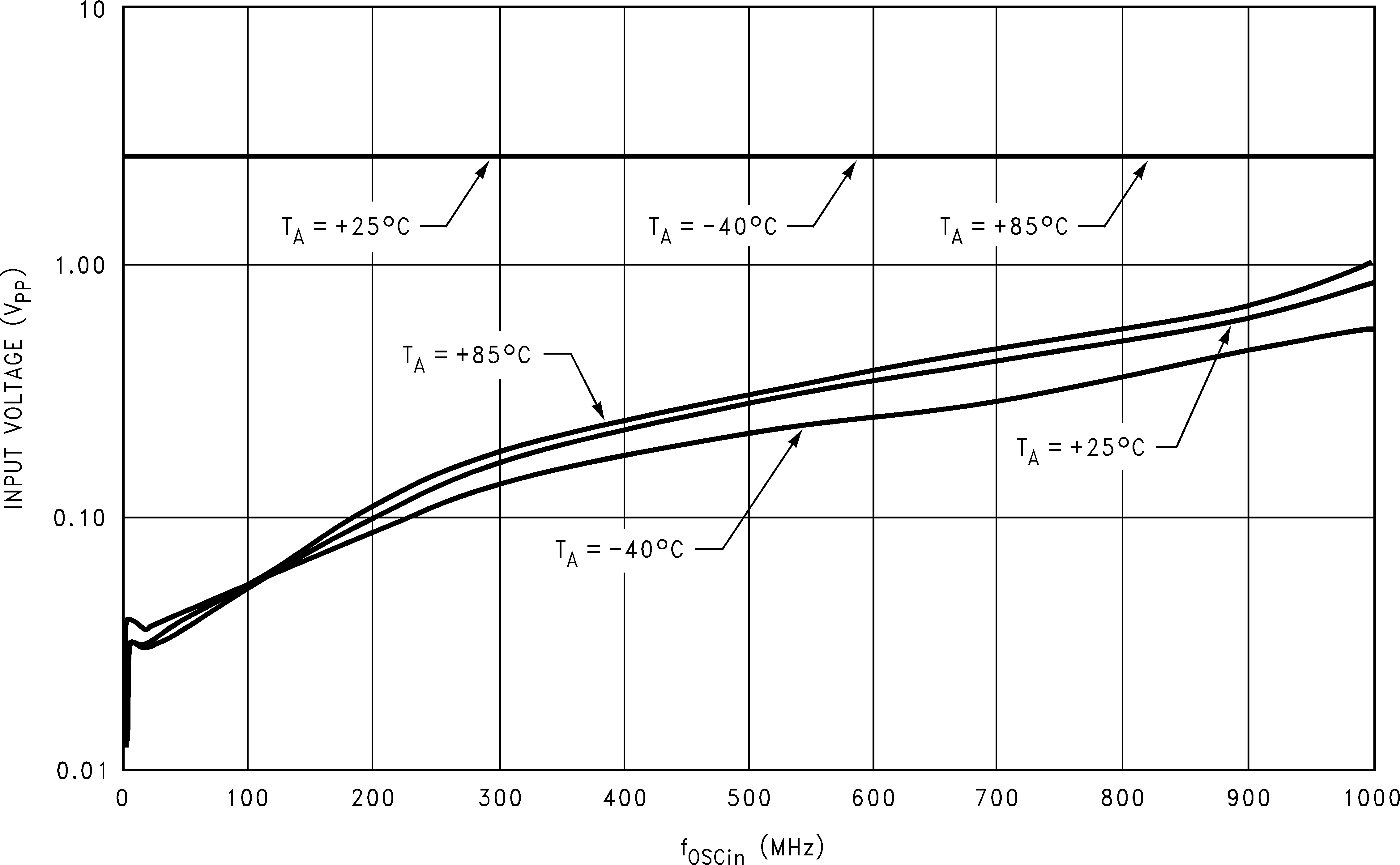
VCC = EN = 2.25 V
Figure 13. LMX243x OSCin Input Voltage vs Frequency
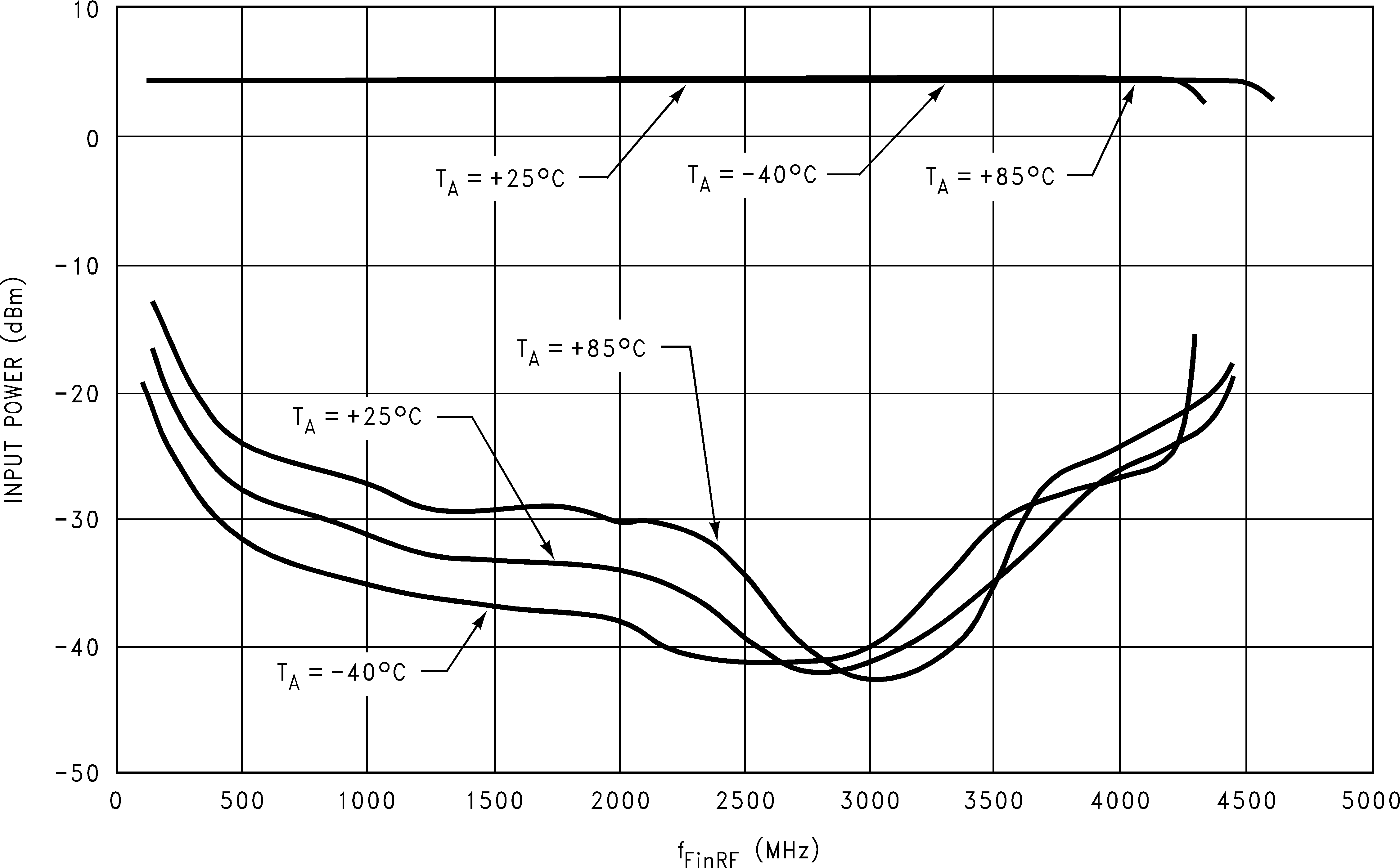
VCC = EN = 2.75 V
Figure 2. LMX2430 FinRF Input Power vs Frequency
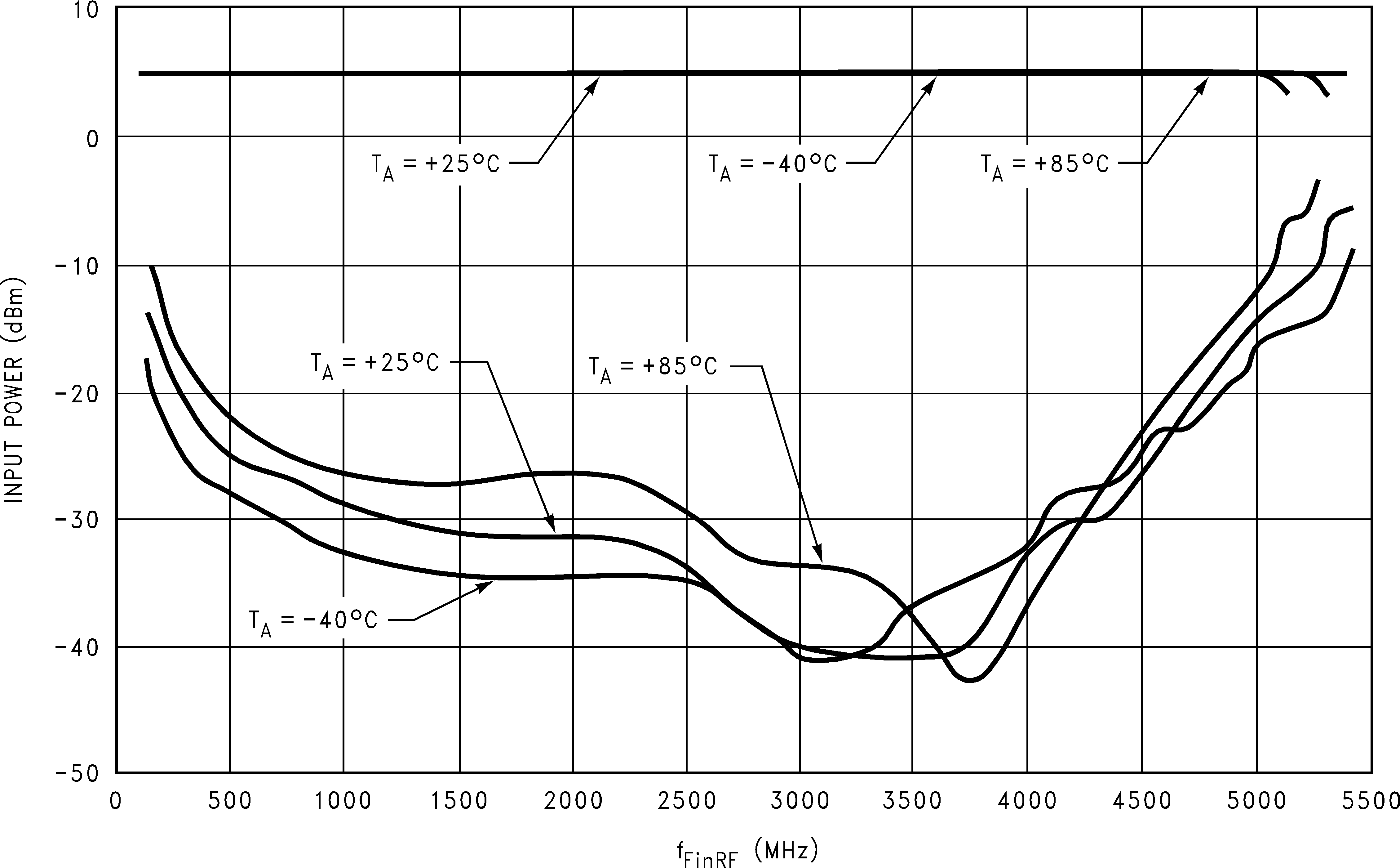
VCC = EN = 2.75 V
Figure 4. LMX2433 FinRF Input Power vs Frequency
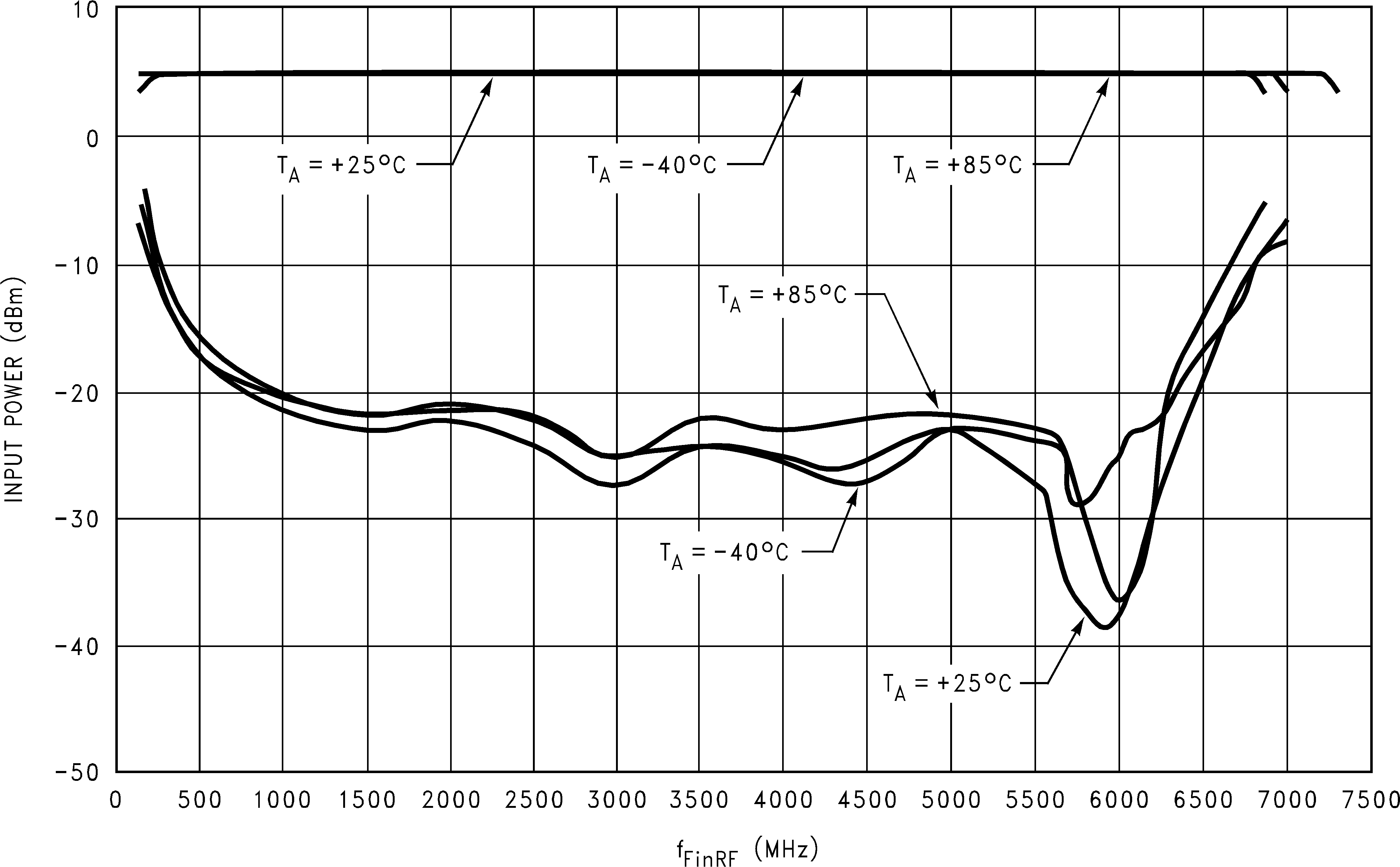
VCC = EN = 2.75 V
Figure 6. LMX2434 FinRF Input Power vs Frequency
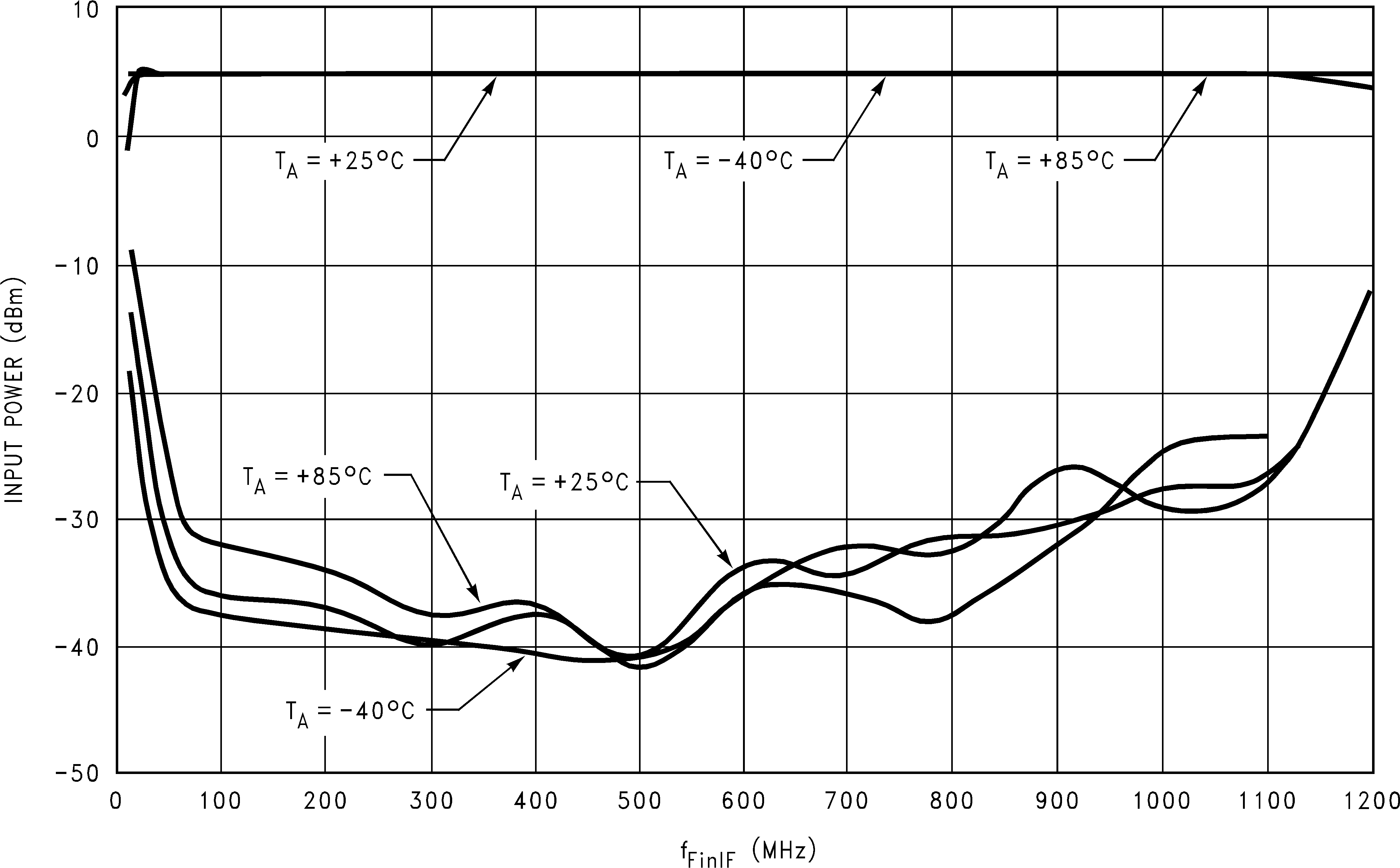
VCC = EN = 2.75 V
Figure 8. LMX2430 FinIF Input Power vs Frequency
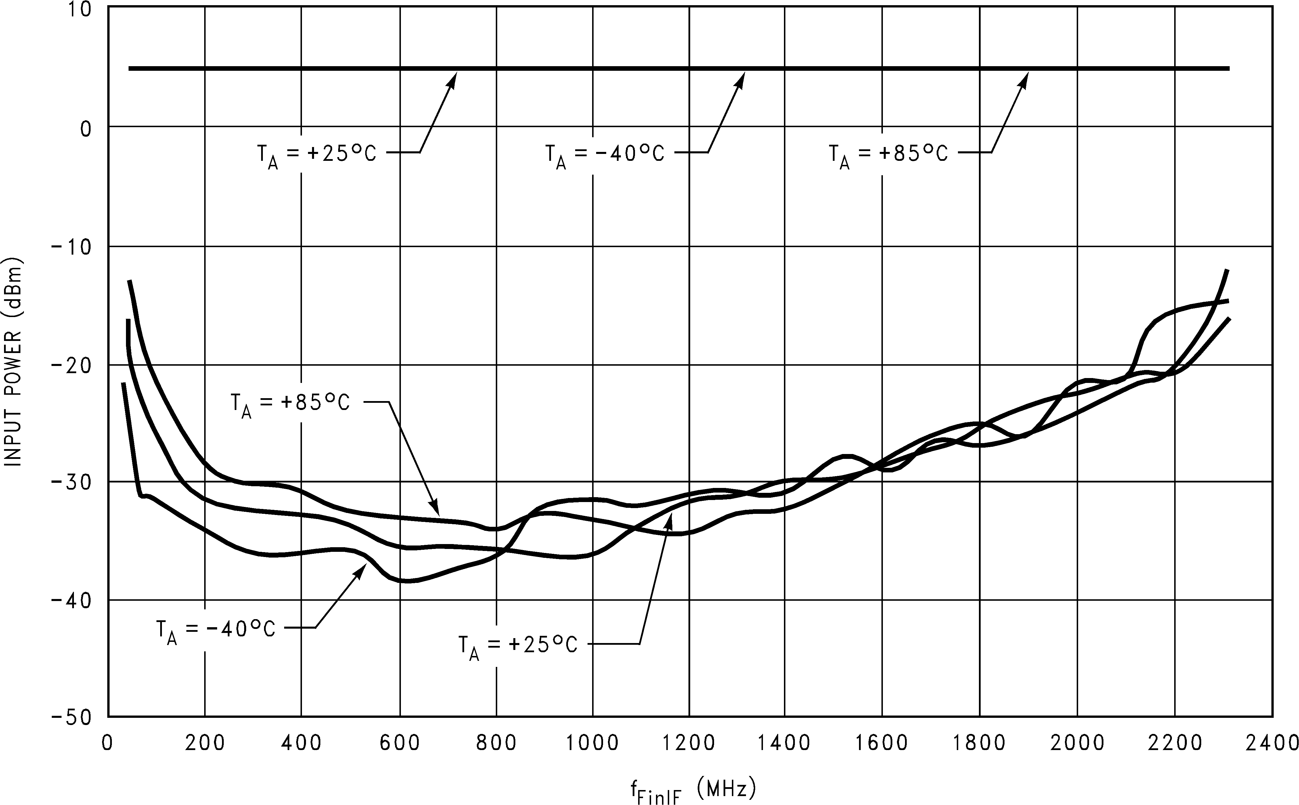
VCC = EN = 2.75 V
Figure 10. LMX2433 FinIF Input Power vs Frequency
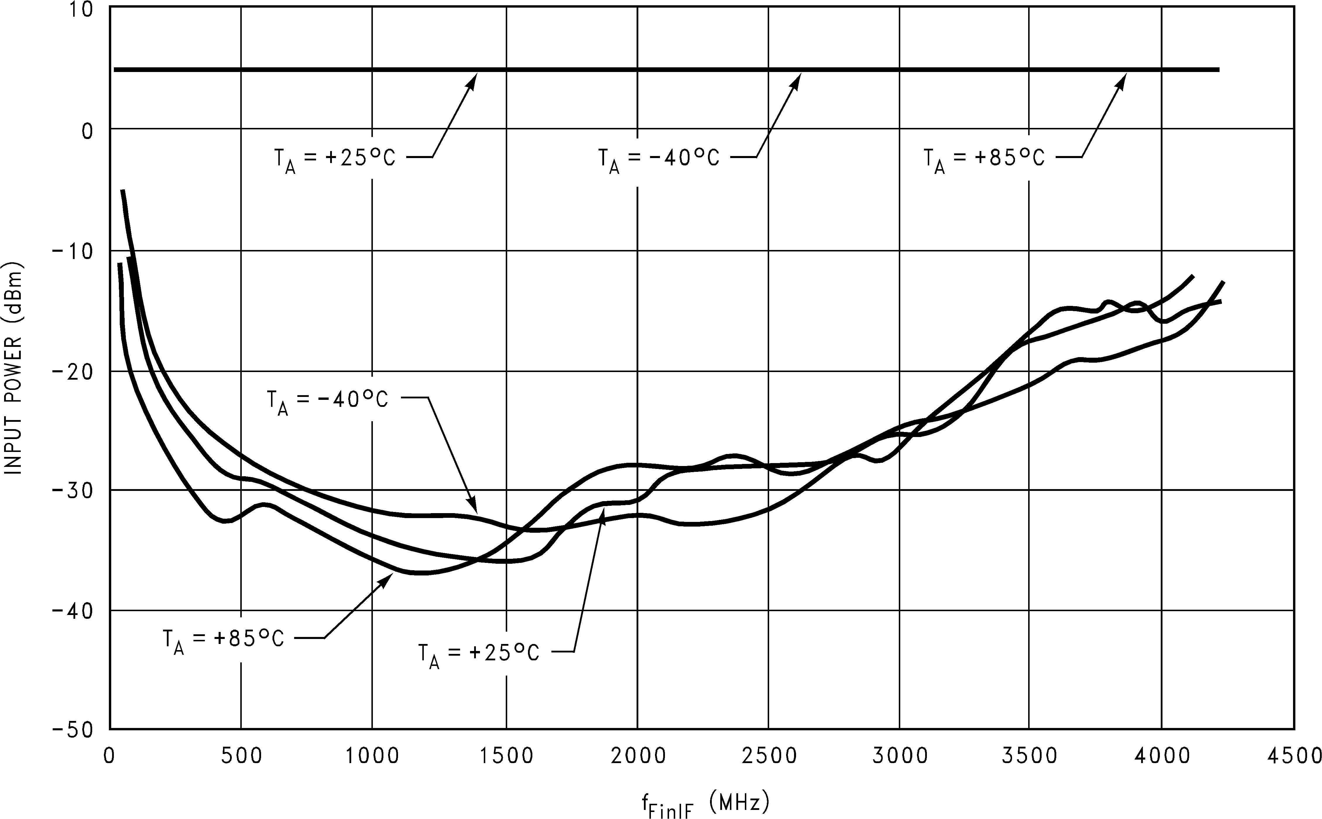
VCC = EN = 2.75 V
Figure 12. LMX2434 FinIF Input Power vs Frequency
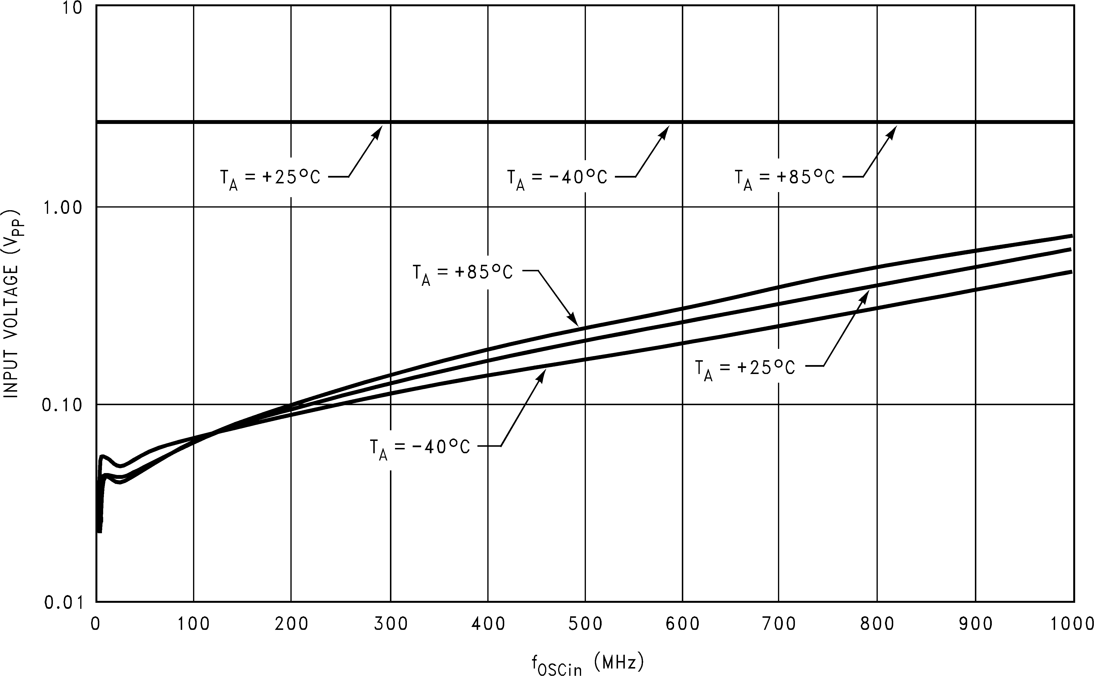
VCC = EN = 2.75 V
Figure 14. LMX243x OSCin Input Voltage vs Frequency
7.6.2 Charge Pump
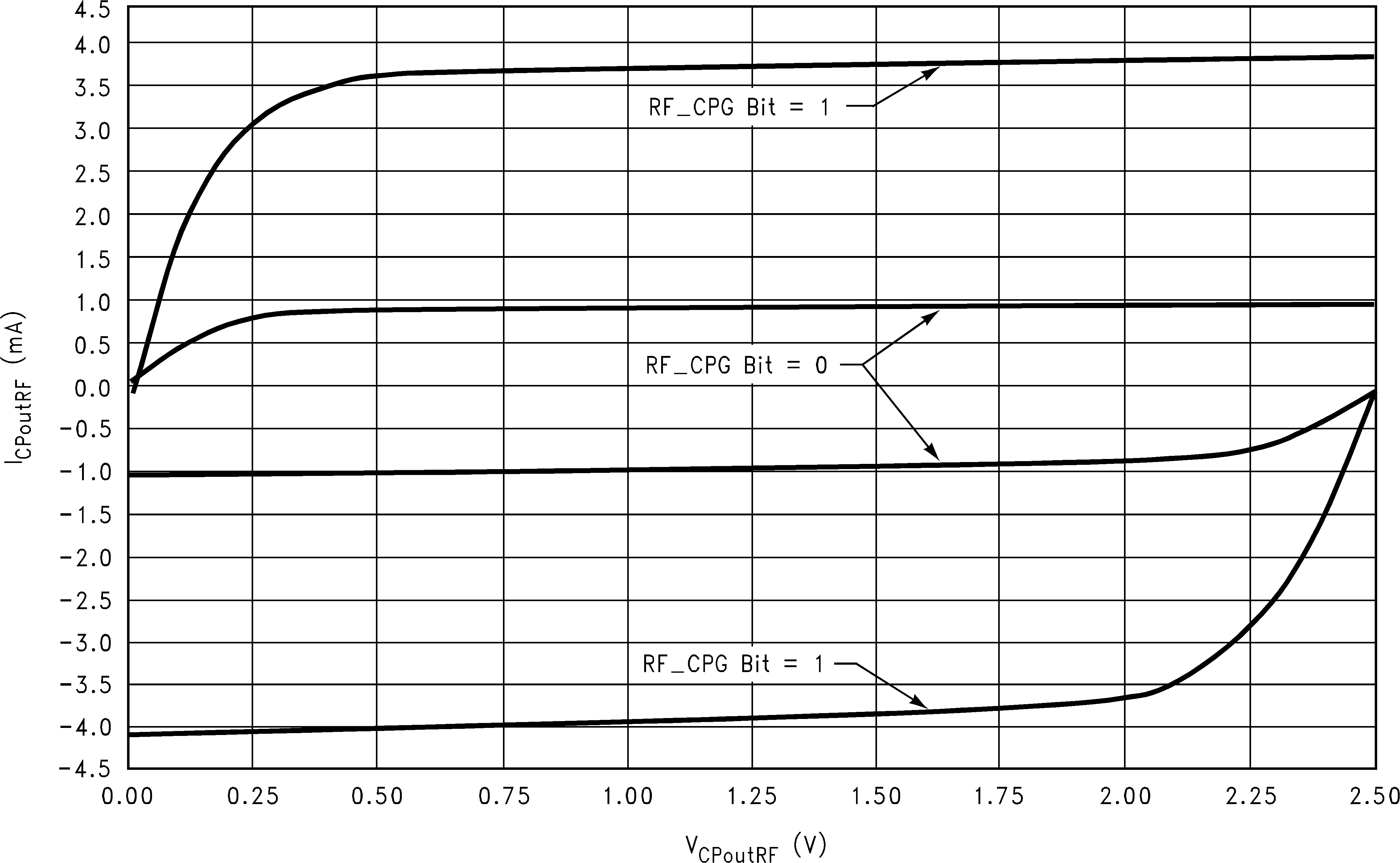
| VCC = EN = 2.5 V | −40°C ≤ TA ≤ +85°C | |
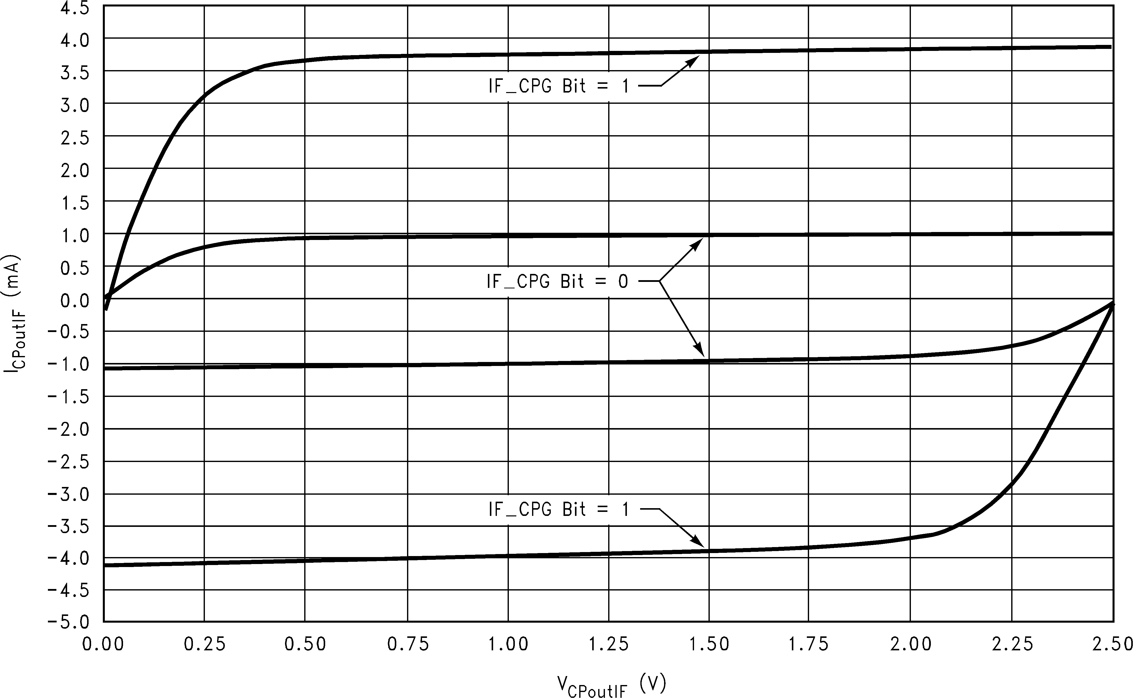
| VCC = EN = 2.5 V | −40°C ≤ TA ≤ +85°C | |
7.6.3 Input Impedance
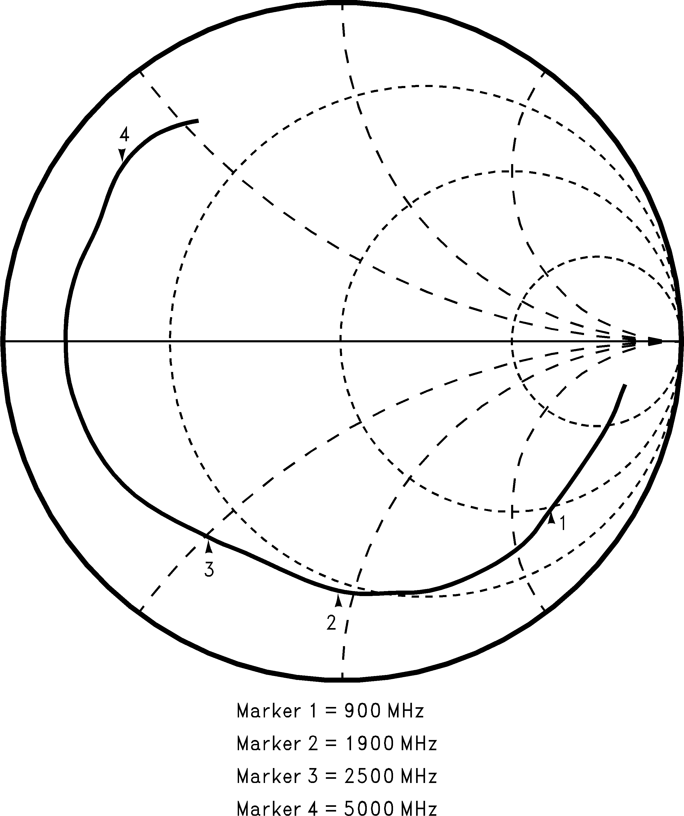
| VCC = EN = 2.5 V | TA = 25°C |
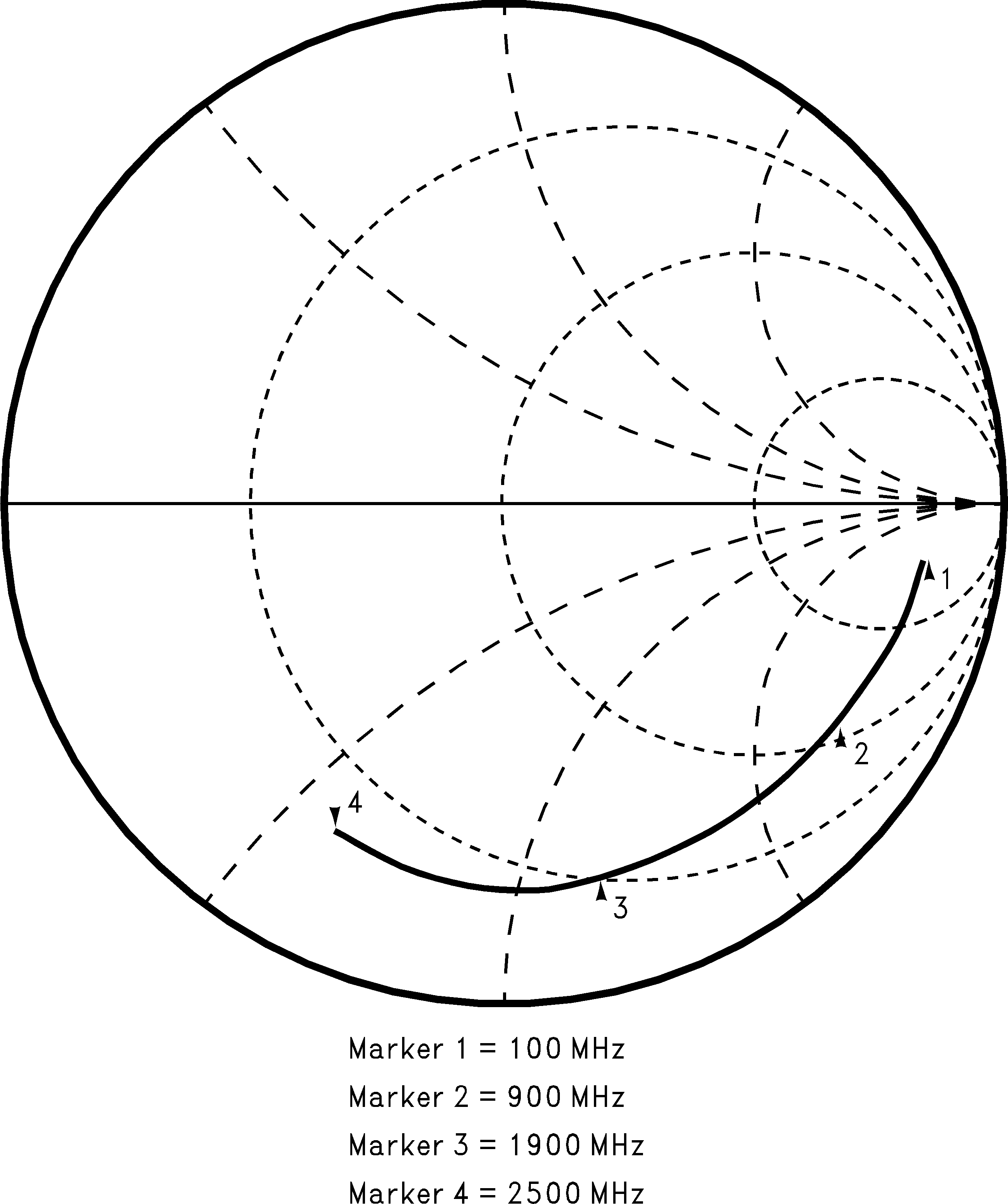
| VCC = EN = 2.5 V | TA = 25°C |
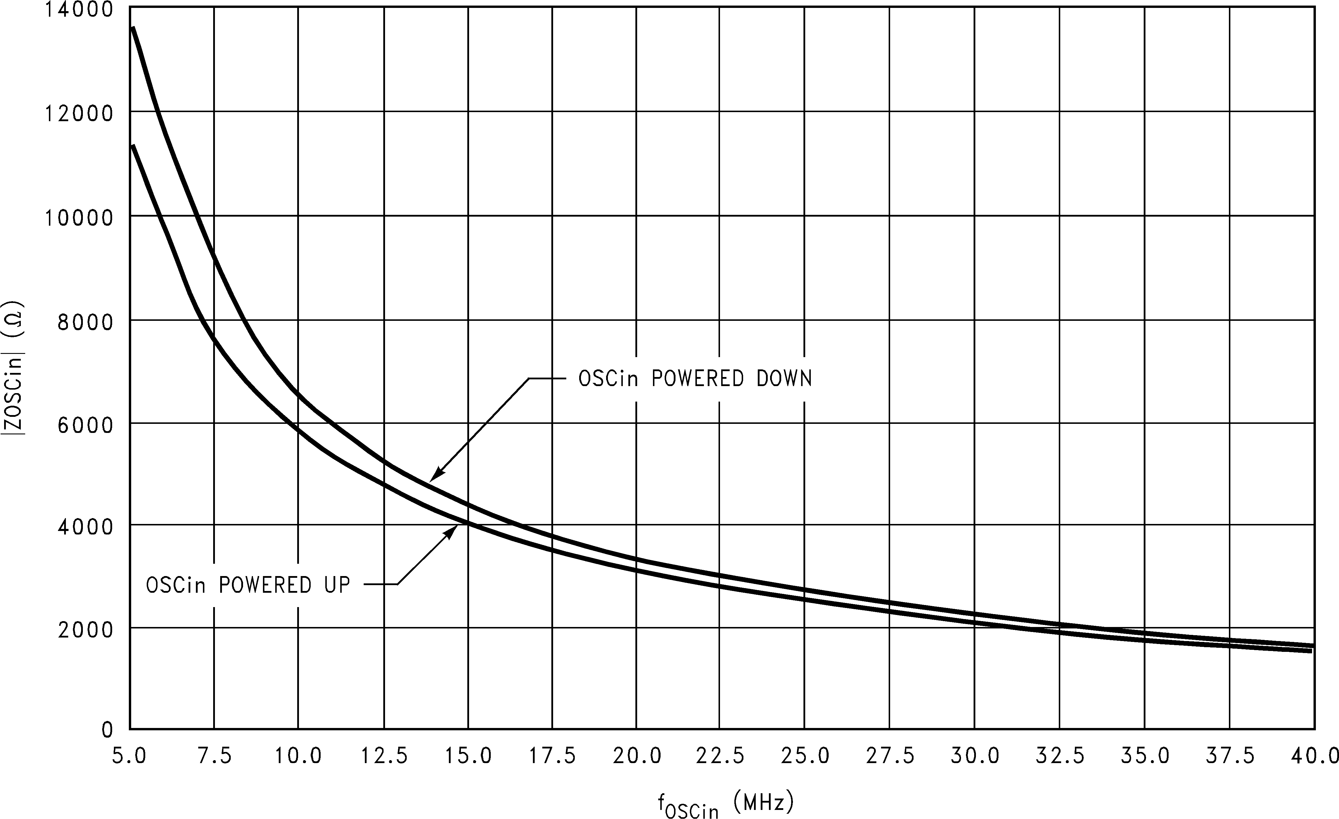
| VCC = EN = 2.5 V | TA = 25°C |

| VCC = EN = 2.5 V | TA = 25°C |
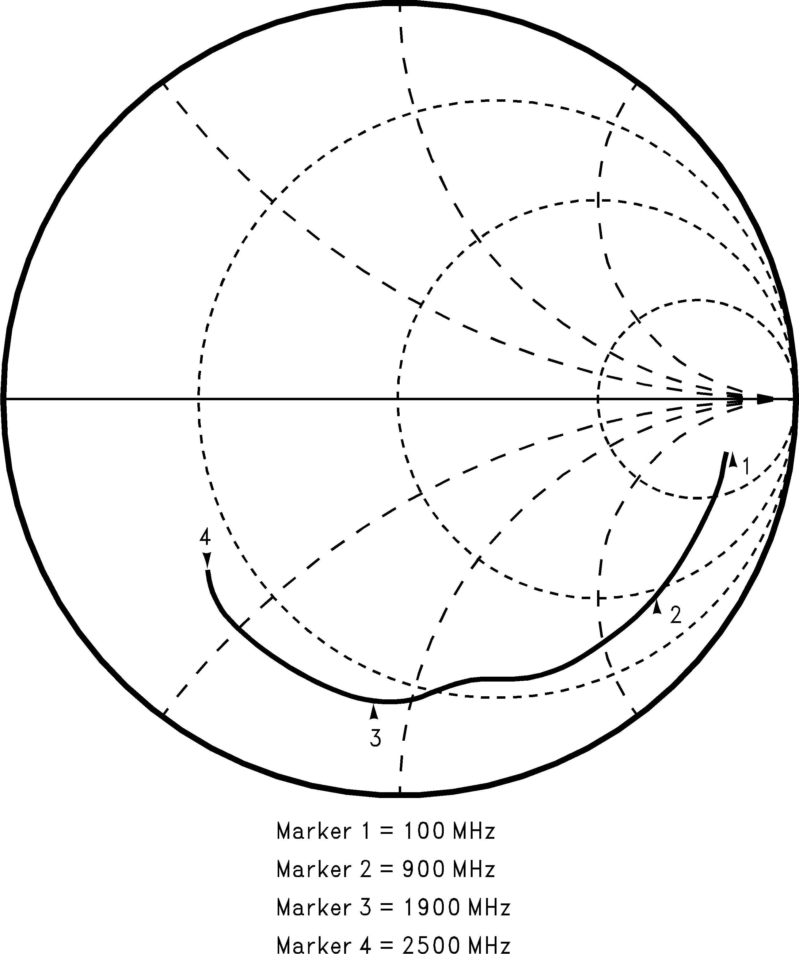
| VCC = EN = 2.5 V | TA = 25°C |

| VCC = EN = 2.5 V | TA = 25°C |