SNAS624B March   2014  – May 2015 LMX2492 , LMX2492-Q1

PRODUCTION DATA.  

  1. Features
  2. Applications
  3. Description
  4. Simplified Schematic
  5. Revision History
  6. Pin Configuration and Functions
  7. Specifications
    1. 7.1 Absolute Maximum Ratings
    2. 7.2 Storage Conditions
    3. 7.3 ESD Ratings
    4. 7.4 Recommended Operating Conditions
    5. 7.5 Thermal Information
    6. 7.6 Electrical Characteristics
    7. 7.7 Timing Requirements, Programming Interface (CLK, DATA, LE)
    8. 7.8 Typical Characteristics
  8. Detailed Description
    1. 8.1  Overview
    2. 8.2  Functional Block Diagram
    3. 8.3  Feature Description
      1. 8.3.1  OSCin Input
      2. 8.3.2  OSCin Doubler
      3. 8.3.3  R Divider
      4. 8.3.4  PLL N Divider
      5. 8.3.5  Fractional Circuitry
      6. 8.3.6  PLL Phase Detector and Charge Pump
      7. 8.3.7  External Loop Filter
      8. 8.3.8  Fastlock and Cycle Slip Reduction
      9. 8.3.9  Lock Detect and Charge Pump Voltage Monitor
        1. 8.3.9.1 Charge Pump Voltage Monitor
        2. 8.3.9.2 Digital Lock Detect
      10. 8.3.10 FSK/PSK Modulation
      11. 8.3.11 Ramping Functions
        1. 8.3.11.1 Ramp Count
        2. 8.3.11.2 Ramp Comparators and Ramp Limits
      12. 8.3.12 Power on Reset (POR)
    4. 8.4  Device Functional Modes
      1. 8.4.1 Continuous Frequency Generator
        1. 8.4.1.1 Integer Mode Operation
        2. 8.4.1.2 Fractional Mode Operation
      2. 8.4.2 Modulated Waveform Generator
    5. 8.5  Programming
      1. 8.5.1 Loading Registers
    6. 8.6  Register Map
    7. 8.7  Register Field Descriptions
      1. 8.7.1 POWERDOWN and Reset Fields
      2. 8.7.2 Dividers and Fractional Controls
        1. 8.7.2.1 Speed Up Controls (Cycle Slip Reduction and Fastlock)
    8. 8.8  Lock Detect and Charge Pump Monitoring
    9. 8.9  TRIG1,TRIG2,MOD, and MUXout Pins
    10. 8.10 Ramping Functions
    11. 8.11 Individual Ramp Controls
  9. Applications and Implementation
    1. 9.1 Application Information
    2. 9.2 Typical Applications
      1. 9.2.1 Design Requirements
      2. 9.2.2 Detailed Design Procedure
      3. 9.2.3 Application Performance Plot - Sawtooth Waveform Example
      4. 9.2.4 Application Performance Plot - Flat Top Triangle Waveform
      5. 9.2.5 Applications Performance Plot -- Complex Triggered Ramp
  10. 10Power Supply Recommendations
  11. 11Layout
    1. 11.1 Layout Guidelines
    2. 11.2 Layout Example
  12. 12Device and Documentation Support
    1. 12.1 Device Support
      1. 12.1.1 Development Support
    2. 12.2 Documentation Support
      1. 12.2.1 Related Documentation
    3. 12.3 Related Links
    4. 12.4 Community Resources
    5. 12.5 Trademarks
    6. 12.6 Electrostatic Discharge Caution
    7. 12.7 Glossary
  13. 13Mechanical, Packaging, and Orderable Information

封装选项

机械数据 (封装 | 引脚)
散热焊盘机械数据 (封装 | 引脚)
订购信息

6 Pin Configuration and Functions

24 Pin WQFN
RTW Package
(Top View)
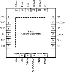
LMX2492 LMX2492-Q1 po_snas624.gif

Pin Functions

PIN I/O DESCRIPTION
NUMBER NAME
0 DAP GND Die Attach Pad. Connect to PCB ground plane.
1 GND GND Ground for charge pump.
2,3 GND GND Ground for Fin Buffer
4,5 Fin
Fin*
Input Complimentary high frequency input pins. Should be AC coupled. If driving single-ended, impedance as seen from Fin and Fin* pins looking outwards from the part should be roughly the same.
6 Vcc Supply Power Supply for Fin Buffer
7 Vcc Supply Supply for On-chip LDOs
8 Vcc Supply Supply for OSCin Buffer
9 OSCin Input Reference Frequency Input
10 GND/
OSCin*
GND/Input Complimentary input for OSCin.
If not used, it is recommended to match the termination as seen from the OSCin terminal looking outwards. However, this may also be grounded as well.
11 GND GND Ground for OSCin Buffer
12 MOD Input/Output Multiplexed Pin for Ramp Triggers, FSK/PSK Modulation, FastLock, Readback, and Diagnostics.
13 CE Input Chip Enable
14 CLK Input Serial Programming Clock.
15 DATA Input Serial Programming Data
16 LE Input Serial Programming Latch Enable
17 MUXout Input/Output Multiplexed Pin for Ramp Triggers, FSK/PSK Modulation, FastLock, Readback, and Diagnostics.
18 Vcc Supply Supply for delta sigma engine.
19 Vcc Supply Supply for general circuitry.
20 TRIG1 Input/Output Multiplexed Pin for Ramp Triggers, FSK/PSK Modulation, FastLock, Readback, and Diagnostics.
21 TRIG2 Input/Output Multiplexed Pin for Ramp Triggers, FSK/PSK Modulation, FastLock, Readback, and Diagnostics.
22 Vcp Supply Power Supply for the charge pump.
23 Rset NC No connect.
24 CPout Output Charge Pump Output