SNOSB31J July 2009 – December 2014 LMX2541
PRODUCTION DATA.
- 1 Features
- 2 Applications
- 3 Description
- 4 Revision History
- 5 Device Comparison Table
- 6 Pin Configuration and Functions
- 7 Specifications
- 8 Parameter Measurement Information
-
9 Detailed Description
- 9.1 Overview
- 9.2 Functional Block Diagrams
- 9.3
Feature Description
- 9.3.1 PLL Reference Oscillator Input Pins
- 9.3.2 PLL R Divider
- 9.3.3 PLL Phase Detector and Charge Pump
- 9.3.4 PLL N Divider and Fractional Circuitry
- 9.3.5 Partially Integrated Loop Filter
- 9.3.6 Low Noise, Fully Integrated VCO
- 9.3.7 Programmable VCO Divider
- 9.3.8 Programmable RF Output Buffer
- 9.3.9 Powerdown Modes
- 9.3.10 Fastlock
- 9.3.11 Lock Detect
- 9.3.12 Current Consumption
- 9.3.13 Fractional Spurs
- 9.3.14 Impact of VCO_DIV on Fractional Spurs
- 9.3.15 PLL Phase Noise
- 9.3.16 Impact of Modulator Order, Dithering, and Larger Equivalent Fractions on Spurs and Phase Noise
- 9.3.17 Modulator Order
- 9.3.18 Programmable Output Power with On/Off
- 9.3.19 Loop Filter
- 9.3.20 Internal VCO Digital Calibration Time
- 9.4 Device Functional Modes
- 9.5 Programming
- 9.6
Register Maps
- 9.6.1
Register R7
- 9.6.1.1 Register R13
- 9.6.1.2 Register R12
- 9.6.1.3 Register R9
- 9.6.1.4 Register R8
- 9.6.1.5 Register R6
- 9.6.1.6 Register R5
- 9.6.1.7
Register R4
- 9.6.1.7.1 OSC_FREQ [7:0] -- OSCin Frequency for VCO Calibration Clocking
- 9.6.1.7.2 VCO_DIV[5:0] - VCO Divider
- 9.6.1.7.3 R3_LF[2:0] -- Value for Internal Loop Filter Resistor R3
- 9.6.1.7.4 R4_LF[2:0] -- Value for Internal Loop Filter Resistor R4
- 9.6.1.7.5 C3_LF[3:0] -- Value for C3 in the Internal Loop Filter
- 9.6.1.7.6 C4_LF[3:0] -- Value for C4 in the Internal Loop Filter
- 9.6.1.8
Register R3
- 9.6.1.8.1 MODE[1:0] -- Operational Mode
- 9.6.1.8.2 Powerdown -- Powerdown Bit
- 9.6.1.8.3 XO - Crystal Oscillator Mode Select
- 9.6.1.8.4 CPG[4:0] -- Charge Pump Current
- 9.6.1.8.5 MUX[3:0] -- Multiplexed Output for Ftest/LD Pin
- 9.6.1.8.6 CPP - Charge Pump Polarity
- 9.6.1.8.7 OSC2X-- OSCin Frequency Doubler
- 9.6.1.8.8 FDM - Extended Fractional Denominator Mode Enable
- 9.6.1.8.9 ORDER[2:0] -- Delta-Sigma Modulator Order
- 9.6.1.8.10 DITH[1:0] -- Dithering
- 9.6.1.8.11 CPT - Charge Pump TRI-STATE
- 9.6.1.8.12 DLOCK[2:0] - Controls for Digital Lock Detect
- 9.6.1.8.13 FSK - Frequency Shift Keying
- 9.6.1.9 Register R2
- 9.6.1.10 Registers R1 and R0
- 9.6.1
Register R7
-
10Application and Implementation
- 10.1
Application Information
- 10.1.1 Determining the Best Frequency Option of the LMX2541 to Use
- 10.1.2 RFout Output Power Test Setup
- 10.1.3 Phase Noise Measurement Test Setup
- 10.1.4 Input and Output Impedance Test Setup
- 10.1.5 ExtVCOin (NOT OSCin) Input Sensitivity Test Setup
- 10.1.6 OSCin Input Sensitivity Test Setup
- 10.1.7 Typical Connections
- 10.2 Typical Application
- 10.1
Application Information
- 11Power Supply Recommendations
- 12Layout
- 13Device and Documentation Support
- 14Mechanical, Packaging, and Orderable Information
8 Parameter Measurement Information
8.1 Bench Test Setups
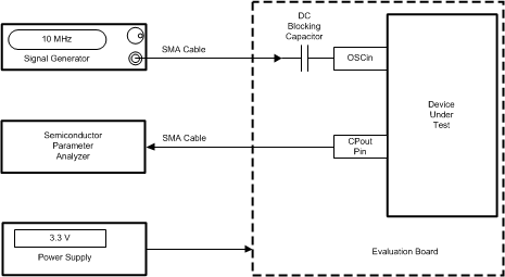
 Figure 22. Charge Pump Currents Test Setup
The charge pump is tested in external VCO mode (MODE=1), although it is no external VCO hooked up. The CPout pin should be disconnected from the any external VCO tuning pin, external loop filter, and also the Vtune pin on the device. A signal is then applied to the OSCin pin to ensure that the R counter is oscillating. This signal does not have to be clean and the frequency is very critical. These currents at the CPout pin are typically measured with a semiconductor parameter analyzer.
8.1.1 Charge Pump Current Measurements
In order to test the TRI-STATE current, the CPT bit is set to one and the current is measured. Aside from having no other sources of leakage attached to this pin, it is also important that the board be well cleaned before doing this test. The temperature and voltage at the charge pump can then be varied and the resulting leakage current is then recorded. Typically, the leakage currents are worst at higher temperatures and higher charge pump voltages.
In order to test the source and sink currents, the CPT bit is set to active mode and the frequency is programmed to something much higher than can be achieved in order to force the charge pump to rail. The reason why this is necessary is that the duty cycle of the charge pump is not 100% unless it is forced against one of the rails. If the charge pump polarity bit (CPP) is set to positive, then the charge pump source current is measured. To measure the sink current, the CPT bit is set to negative. The part is then programmed and the charge pump will rail in one direction. The semiconductor parameter analyzer measures the current at a particular charge pump voltage. The phase detector polarity bit, CPP, can be toggled to test between the negative and positive charge pump gains. In order to test leakage, set the TRI-STATE bit, CPT, to 1 so that this can be measured. For the most accurate measurements, it is desirable that the CPout and Vtune pin are not shorted together for these measurements. Once these currents are measured, then the datasheet parameters can be calculated.
A summary of these charge pump tests is given in the table below.
| MEASUREMENT | PLL_R | PLL_N | CPG | CPT | CPP |
|---|---|---|---|---|---|
| Leakage Current | X | X | X | 1 (TRI-STATE) | X |
| Source Current | 1 | 4000 | 0 - 31 | 0 (Active) | 1 (Positive) |
| Sink Current | 1 | 4000 | 0 - 31 | 0 (Active) | 0 (Negative) |
8.1.2 Charge Pump Current Definitions
8.1.2.1 Charge Pump Current Definitions

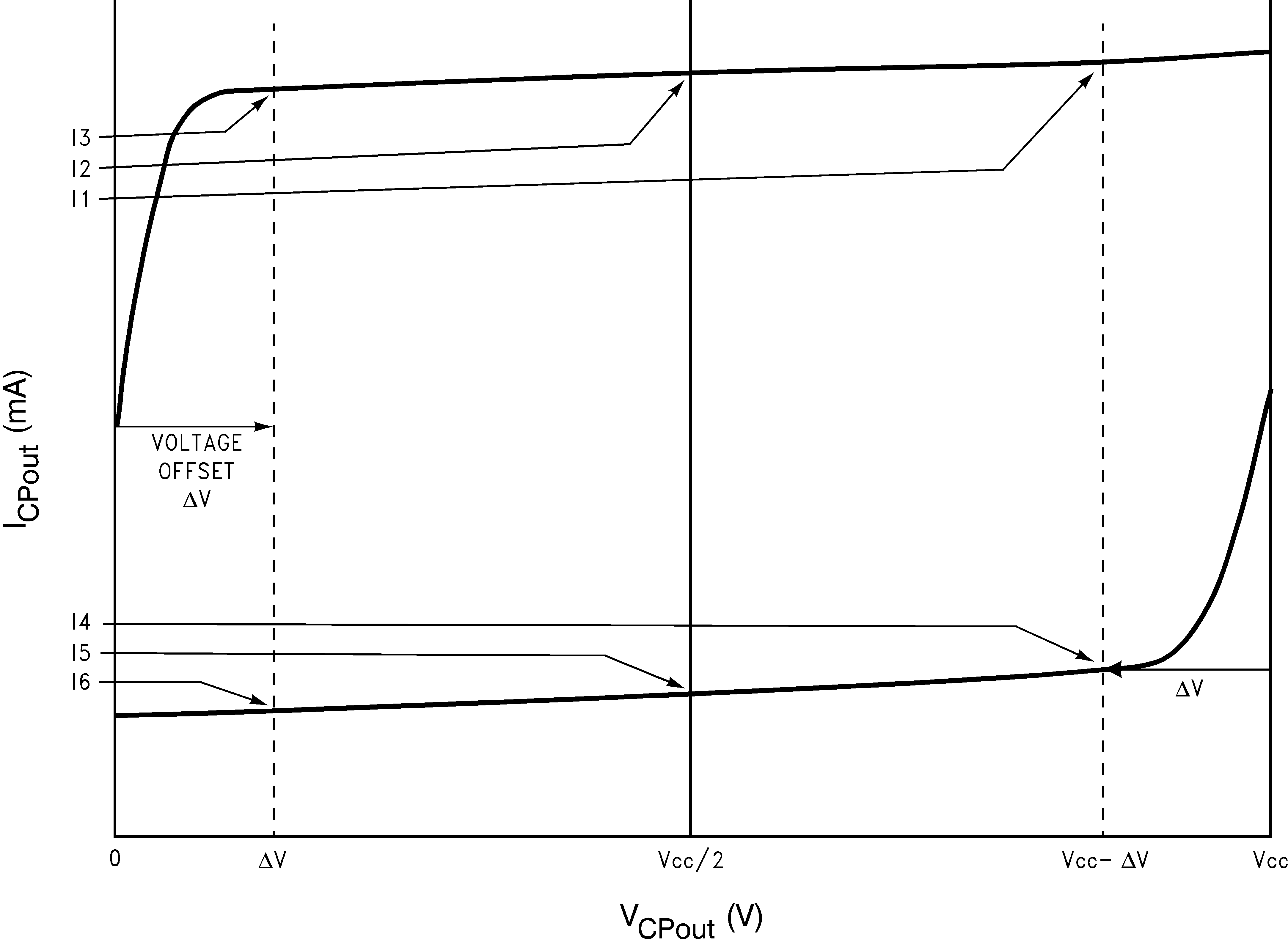
I1 = Charge Pump Sink Current at VCPout = Vcc - ΔV
I2 = Charge Pump Sink Current at VCPout = Vcc/2
I3 = Charge Pump Sink Current at VCPout = ΔV
I4 = Charge Pump Source Current at VCPout = Vcc - ΔV
I5 = Charge Pump Source Current at VCPout = Vcc/2
I6 = Charge Pump Source Current at VCPout = ΔV
ΔV = Voltage offset from the positive and negative supply rails. Defined to be 0.4 volts for this part.
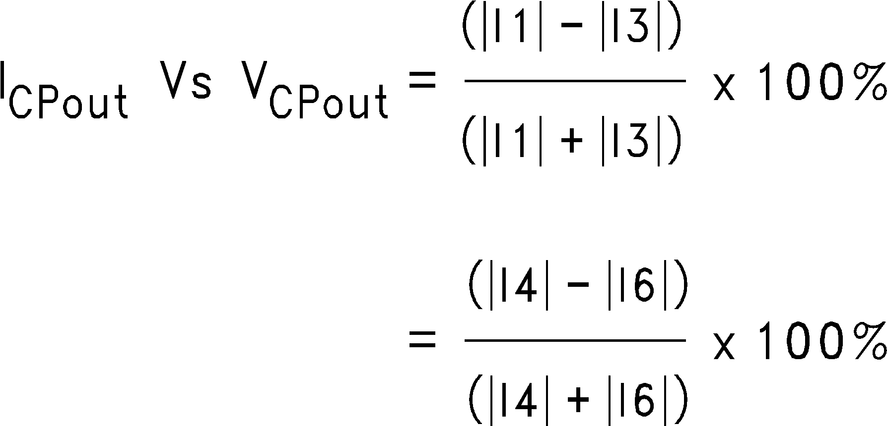
8.1.2.2 Variation of Charge Pump Current Magnitude vs. Charge Pump Voltage

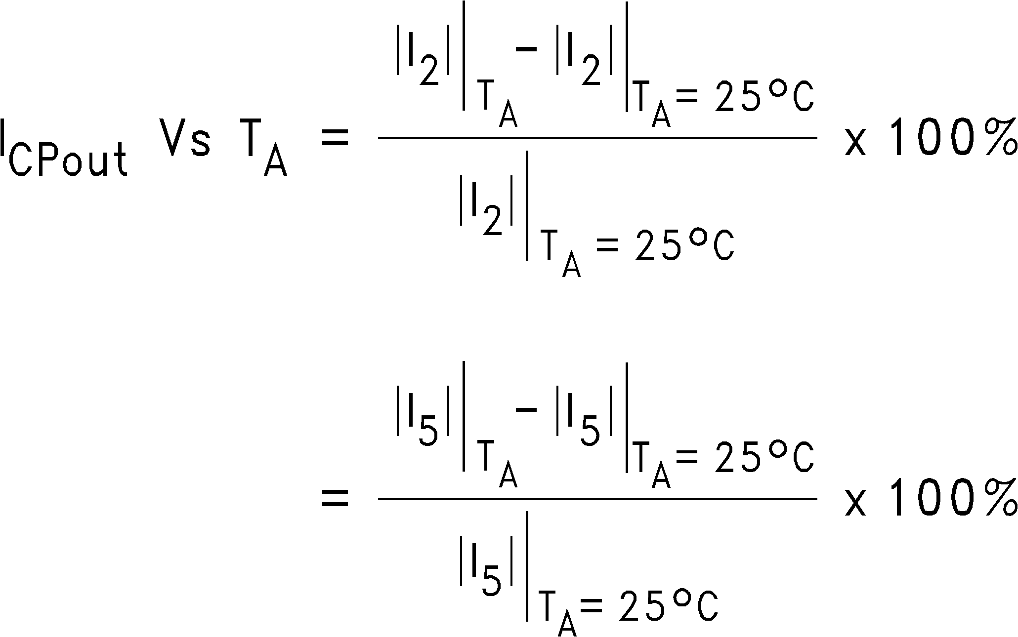
8.1.2.3 Variation of Charge Pump Current Magnitude vs. Temperature

 Figure 23. Charge Pump Sink vs. Source Current Mismatch