ZHCSP40B October 2021 – June 2022 LMX2571-EP
PRODUCTION DATA
- 1 特性
- 2 应用
- 3 说明
- 4 Revision History
- 5 Pin Configuration and Functions
- 6 Specifications
-
7 Detailed Description
- 7.1 Overview
- 7.2 Functional Block Diagram
- 7.3
Feature Description
- 7.3.1 Differences Between the LMX2571 and LMX2571-EP
- 7.3.2 Reference Oscillator Input
- 7.3.3 R-Dividers and Multiplier
- 7.3.4 PLL Phase Detector and Charge Pump
- 7.3.5 PLL N-Divider and Fractional Circuitry
- 7.3.6 Partially Integrated Loop Filter
- 7.3.7 Low-Noise, Fully Integrated VCO
- 7.3.8 External VCO Support
- 7.3.9 Programmable RF Output Divider
- 7.3.10 Programmable RF Output Buffer
- 7.3.11 Integrated TX, RX Switch
- 7.3.12 Power Down
- 7.3.13 Lock Detect
- 7.3.14 FSK Modulation
- 7.3.15 FastLock
- 7.3.16 Register Readback
- 7.4 Device Functional Modes
- 7.5 Programming
- 7.6
Register Maps
- 7.6.1 R60 Register (offset = 3Ch) [reset = 4000h]
- 7.6.2 R58 Register (offset = 3Ah) [reset = C00h]
- 7.6.3 R53 Register (offset = 35h) [reset = 2802h]
- 7.6.4 R47 Register (offset = 2Fh) [reset = 0h]
- 7.6.5 R46 Register (offset = 2Eh) [reset = 1Ah]
- 7.6.6 R42 Register (offset = 2Ah) [reset = 210h]
- 7.6.7 R41 Register (offset = 29h) [reset = 810h]
- 7.6.8 R40 Register (offset = 28h) [reset = 101Ch]
- 7.6.9 R39 Register (offset = 27h) [reset = 11F0h]
- 7.6.10 R35 Register (offset = 23h) [reset = 647h]
- 7.6.11 R34 Register (offset = 22h) [reset = 1000h]
- 7.6.12 R33 Register (offset = 21h) [reset = 0h]
- 7.6.13 R25 to R32 Register (offset = 19h to 20h) [reset = 0h]
- 7.6.14 R24 Register (offset = 18h) [reset = 10h]
- 7.6.15 R23 Register (offset = 17h) [reset = 10A4h]
- 7.6.16 R22 Register (offset = 16h) [reset = 8584h]
- 7.6.17 R21 Register (offset = 15h) [reset = 101h]
- 7.6.18 R20 Register (offset = 14h) [reset = 28h]
- 7.6.19 R19 Register (offset = 13h) [reset = 0h]
- 7.6.20 R18 Register (offset = 12h) [reset = 0h]
- 7.6.21 R17 Register (offset = 11h) [reset = 0h]
- 7.6.22 R9 to R16 Register (offset = 9h to 10h) [reset = 0h]
- 7.6.23 R8 Register (offset = 8h) [reset = 10h]
- 7.6.24 R7 Register (offset = 7h) [reset = 10A4h]
- 7.6.25 R6 Register (offset = 6h) [reset = 8584h]
- 7.6.26 R5 Register (offset = 5h) [reset = 101h]
- 7.6.27 R4 Register (offset = 4h) [reset = 28h]
- 7.6.28 R3 Register (offset = 3h) [reset = 0h]
- 7.6.29 R2 Register (offset = 2h) [reset = 0h]
- 7.6.30 R1 Register (offset = 1h) [reset = 0h]
- 7.6.31 R0 Register (offset = 0h) [reset = 3h]
-
8 Application and Implementation
- 8.1
Application Information
- 8.1.1 Direct Digital FSK Modulation
- 8.1.2 Frequency and Output Port Switching
- 8.1.3 OSCin Configuration
- 8.1.4 Register R0 F1F2_INIT, F1F2_MODE Usage
- 8.1.5 FastLock With External VCO
- 8.1.6 OSCin Slew Rate
- 8.1.7 RF Output Buffer Power Control
- 8.1.8 RF Output Buffer Type
- 8.1.9 MULT Multiplier
- 8.1.10 Integrated VCO
- 8.2 Typical Applications
- 8.3 Do's and Don'ts
- 8.1
Application Information
- 9 Power Supply Recommendations
- 10Layout
- 11Device and Documentation Support
- 12Mechanical, Packaging, and Orderable Information
8.1.8 RF Output Buffer Type
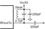
Registers R35, OUTBUF_TX_TYPE, OUTBUF_RX_TYPE are used to configure the RF output buffer type between open drain and push-pull. Push-pull is easy to use; all that is required is a DC-blocking capacitor at the output. The output waveform is square wave and therefore, harmonics rich. Open-drain output provides an option to reduce the harmonics using an LC resonant pullup network at its output. Table 8-5 summarizes an example an open-drain vs. push-pull application.
Table 8-5 RF Output Buffer Type
| BUFFER TYPE | OPEN-DRAIN | PUSH-PULL | ||||
|---|---|---|---|---|---|---|
| Connection Diagram |  |  | ||||
| Output Power | 470 MHz | 480 MHz | 490 MHz | 470 MHz | 480 MHz | 490 MHz |
| fo | 2.7 dBm | 2.8 dBm | 2.8 dBm | –0.1 dBm | 0 dBm | 0.1 dBm |
| 2fo | –31 dBc | –30.7 dBc | –30.5 dBc | –30.4 dBc | –30.2 dBc | –30 dBc |
| 3fo | –17.3 dBc | –17.9 dBc | –18.1 dBc | –11.9 dBc | –12.1 dBc | –12.4 dBc |
| 4fo | –39 dBc | –40.4 dBc | –41.6 dBc | –28.5 dBc | –28.4 dBc | –28.1 dBc |
| 5fo | –18.1 dBc | –17.8 dBc | –17.6 dBc | –15.6 dBc | –15.6 dBc | –15.7 dBc |
| 6fo | –27.6 dBc | –27.2 dBc | –28.5 dBc | –29.5 dBc | –29.8 dBc | –29.3 dBc |
Clearly, with a proper LC pull up in open-drain architecture, the 3rd to 5th harmonics could be reduced.