ZHCSP40B October 2021 – June 2022 LMX2571-EP
PRODUCTION DATA
- 1 特性
- 2 应用
- 3 说明
- 4 Revision History
- 5 Pin Configuration and Functions
- 6 Specifications
-
7 Detailed Description
- 7.1 Overview
- 7.2 Functional Block Diagram
- 7.3
Feature Description
- 7.3.1 Differences Between the LMX2571 and LMX2571-EP
- 7.3.2 Reference Oscillator Input
- 7.3.3 R-Dividers and Multiplier
- 7.3.4 PLL Phase Detector and Charge Pump
- 7.3.5 PLL N-Divider and Fractional Circuitry
- 7.3.6 Partially Integrated Loop Filter
- 7.3.7 Low-Noise, Fully Integrated VCO
- 7.3.8 External VCO Support
- 7.3.9 Programmable RF Output Divider
- 7.3.10 Programmable RF Output Buffer
- 7.3.11 Integrated TX, RX Switch
- 7.3.12 Power Down
- 7.3.13 Lock Detect
- 7.3.14 FSK Modulation
- 7.3.15 FastLock
- 7.3.16 Register Readback
- 7.4 Device Functional Modes
- 7.5 Programming
- 7.6
Register Maps
- 7.6.1 R60 Register (offset = 3Ch) [reset = 4000h]
- 7.6.2 R58 Register (offset = 3Ah) [reset = C00h]
- 7.6.3 R53 Register (offset = 35h) [reset = 2802h]
- 7.6.4 R47 Register (offset = 2Fh) [reset = 0h]
- 7.6.5 R46 Register (offset = 2Eh) [reset = 1Ah]
- 7.6.6 R42 Register (offset = 2Ah) [reset = 210h]
- 7.6.7 R41 Register (offset = 29h) [reset = 810h]
- 7.6.8 R40 Register (offset = 28h) [reset = 101Ch]
- 7.6.9 R39 Register (offset = 27h) [reset = 11F0h]
- 7.6.10 R35 Register (offset = 23h) [reset = 647h]
- 7.6.11 R34 Register (offset = 22h) [reset = 1000h]
- 7.6.12 R33 Register (offset = 21h) [reset = 0h]
- 7.6.13 R25 to R32 Register (offset = 19h to 20h) [reset = 0h]
- 7.6.14 R24 Register (offset = 18h) [reset = 10h]
- 7.6.15 R23 Register (offset = 17h) [reset = 10A4h]
- 7.6.16 R22 Register (offset = 16h) [reset = 8584h]
- 7.6.17 R21 Register (offset = 15h) [reset = 101h]
- 7.6.18 R20 Register (offset = 14h) [reset = 28h]
- 7.6.19 R19 Register (offset = 13h) [reset = 0h]
- 7.6.20 R18 Register (offset = 12h) [reset = 0h]
- 7.6.21 R17 Register (offset = 11h) [reset = 0h]
- 7.6.22 R9 to R16 Register (offset = 9h to 10h) [reset = 0h]
- 7.6.23 R8 Register (offset = 8h) [reset = 10h]
- 7.6.24 R7 Register (offset = 7h) [reset = 10A4h]
- 7.6.25 R6 Register (offset = 6h) [reset = 8584h]
- 7.6.26 R5 Register (offset = 5h) [reset = 101h]
- 7.6.27 R4 Register (offset = 4h) [reset = 28h]
- 7.6.28 R3 Register (offset = 3h) [reset = 0h]
- 7.6.29 R2 Register (offset = 2h) [reset = 0h]
- 7.6.30 R1 Register (offset = 1h) [reset = 0h]
- 7.6.31 R0 Register (offset = 0h) [reset = 3h]
-
8 Application and Implementation
- 8.1
Application Information
- 8.1.1 Direct Digital FSK Modulation
- 8.1.2 Frequency and Output Port Switching
- 8.1.3 OSCin Configuration
- 8.1.4 Register R0 F1F2_INIT, F1F2_MODE Usage
- 8.1.5 FastLock With External VCO
- 8.1.6 OSCin Slew Rate
- 8.1.7 RF Output Buffer Power Control
- 8.1.8 RF Output Buffer Type
- 8.1.9 MULT Multiplier
- 8.1.10 Integrated VCO
- 8.2 Typical Applications
- 8.3 Do's and Don'ts
- 8.1
Application Information
- 9 Power Supply Recommendations
- 10Layout
- 11Device and Documentation Support
- 12Mechanical, Packaging, and Orderable Information
8.1.5 FastLock With External VCO
Fastlock may be required in PLL mode where an external VCO with a narrow loop bandwidth is desired. The LMX2571-EP adopts a new FastLock approach to support the very fast switching time requirement in PLL mode.
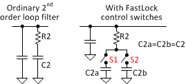
There are two control pins in the chip, FLout1 and FLout2. Each pin is used to control a SPST analog switch, S1 and S2. The loop filter value with or without FastLock is the same, except that with FastLock, one more C2 and two SPST switches are needed.
 Figure 8-7 FastLock With SPST Switches
When LMX2571-EP is locked to F1, FLout1 will close the switch S1. When the LMX2571-EP is locked to F2, the user can program the F1F2_SEL bit in the R0 register to release the switch S1 while the FLout2 closes the S2. Although S1 is released, the charge stored in C2a remains unchanged. Thus, when the output is switched back to F1, the Vtune voltage is almost correct, no (or little) charging or discharging to C2a is required which speeds up the switching time. For example, if Vtune for F1 and F2 are 1 V and 2 V, respectively, without FastLock, when the switching frequency shifts from F1 to F2, C2 will have to be re-charged from 1 V to 2 V — this is a big voltage jump. With FastLock, when S2 is closed, Vtune is almost equal to 2 V because C2b maintains the charge. Only a tiny voltage jump (re-charge) is required to make it reach the final Vtune voltage.
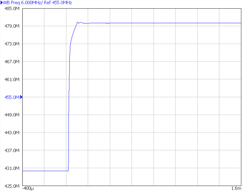
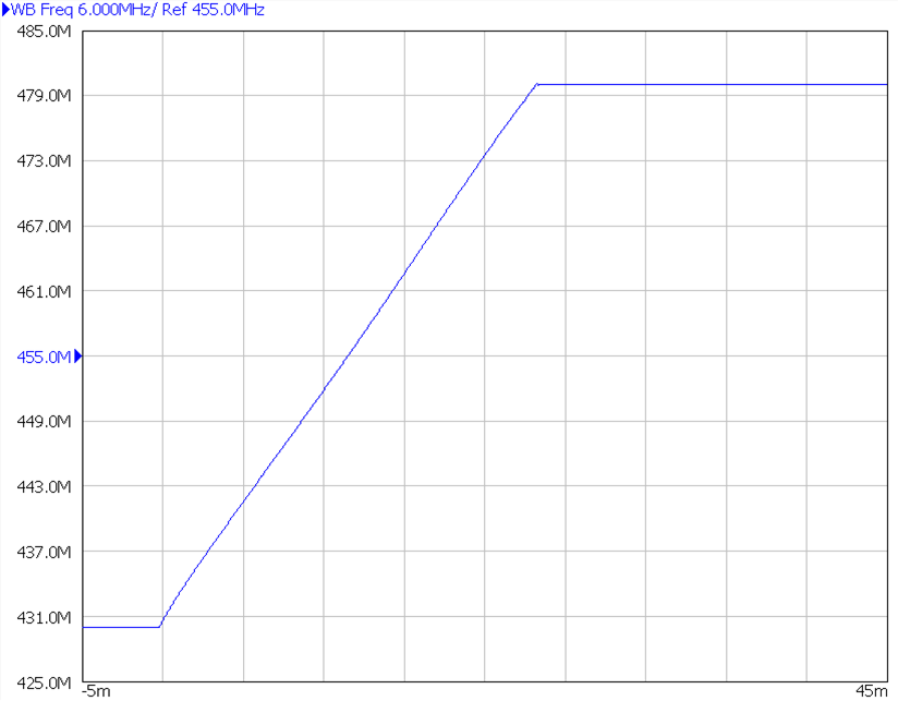
Figure 8-8 and Figure 8-9 compare the frequency switching time using different switching methods. In both cases, the loop bandwidth is 4 kHz while fPD is 28 MHz. Figure 8-8 shows the switching time for a frequency jump from 430 MHz to 480 MHz with SPST switches. Frequency switching is toggled by the F1F2_SEL bit. Switching time is approximately 1 ms. Frequency switching in Figure 8-9 is done in the traditional way. That is, change the output frequency by writing to the relevant registers such as N-divider values. In this case, because fPD is very much bigger than the loop bandwidth, cycle slipping jeopardizes the switching time to more than 20 ms.
 Figure 8-8 F1F2 Switching With SPST Switches
 Figure 8-9 Change F1 Frequency Through SPI Programming