ZHCSGL5C March 2017 – April 2019 LMX2594
PRODUCTION DATA.
- 1 特性
- 2 应用
- 3 说明
- 4 修订历史记录
- 5 Pin Configuration and Functions
- 6 Specifications
-
7 Detailed Description
- 7.1 Overview
- 7.2 Functional Block Diagram
- 7.3
Feature Description
- 7.3.1 Reference Oscillator Input
- 7.3.2 Reference Path
- 7.3.3 PLL Phase Detector and Charge Pump
- 7.3.4 N-Divider and Fractional Circuitry
- 7.3.5 MUXout Pin
- 7.3.6 VCO (Voltage-Controlled Oscillator)
- 7.3.7 Channel Divider
- 7.3.8 Output Buffer
- 7.3.9 Power-Down Modes
- 7.3.10 Phase Synchronization
- 7.3.11 Phase Adjust
- 7.3.12 Fine Adjustments for Phase Adjust and Phase SYNC
- 7.3.13 Ramping Function
- 7.3.14 SYSREF
- 7.3.15 SysRefReq Pin
- 7.4 Device Functional Modes
- 7.5 Programming
- 7.6
Register Maps
- 7.6.1 General Registers R0, R1, & R7
- 7.6.2 Input Path Registers
- 7.6.3 Charge Pump Registers (R13, R14)
- 7.6.4 VCO Calibration Registers
- 7.6.5 N Divider, MASH, and Output Registers
- 7.6.6 SYNC and SysRefReq Input Pin Register
- 7.6.7 Lock Detect Registers
- 7.6.8 MASH_RESET
- 7.6.9 SysREF Registers
- 7.6.10 CHANNEL Divider Registers
- 7.6.11 Ramping and Calibration Fields
- 7.6.12 Ramping Registers
- 7.6.13 Readback Registers
- 8 Application and Implementation
- 9 Power Supply Recommendations
- 10Layout
- 11器件和文档支持
- 12机械、封装和可订购信息
6.6 Timing Requirements
(3.15 V ≤ VCC ≤ 3.45 V, –40°C ≤ TA ≤ +85°C, except as specified. Nominal values are at VCC = 3.3 V, TA = 25°C)| MIN | NOM | MAX | UNIT | |||
|---|---|---|---|---|---|---|
| SYNC, SYSRefReq, RampClk, and RampDIR Pins | ||||||
| tSETUP | Setup time for pin relative to OSCin rising edge | SYNC pin | 2.5 | ns | ||
| SysRefReq pin | 2.5 | |||||
| tHOLD | Hold time for SYNC pin relative to OSCin rising edge | SYNC pin | 2 | ns | ||
| SysRefReq pin | 2 | |||||
| DIGITAL INTERFACE WRITE SPECIFICATIONS | ||||||
| fSPIWrite | SPI write speed | tCWL + tCWH > 13.333 ns | 75 | MHz | ||
| tCE | Clock to enable low time | See Figure 1 | 5 | ns | ||
| tDCS | Data to clock setup time | 2 | ns | |||
| tCDH | Clock to data hold time | 2 | ns | |||
| tCWH | Clock pulse width high | 5 | ns | |||
| tCWL | Clock pulse width low | 5 | ns | |||
| tECS | Enable to clock setup time | 5 | ns | |||
| tEWH | Enable pulse width high | 2 | ns | |||
| DIGITAL INTERFACE READBACK SPECIFICATIONS | ||||||
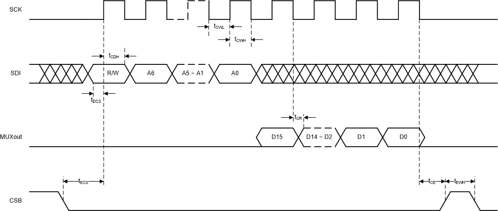
| fSPIReadback | SPI readback speed | See Figure 2 | 50 | MHz | ||
| tCE | Clock to enable low time | 10 | ns | |||
| tDCS | Data to clock setup time | 2 | ns | |||
| tCDH | Clock to data hold time | 2 | ns | |||
| tCR | Clock falling edge to available readback data wait time. | 0 | 10 | ns | ||
| tCWH | Clock pulse width high | 10 | ns | |||
| tCWL | Clock pulse width low | 10 | ns | |||
| tECS | Enable to clock setup time | 10 | ns | |||
| tEWH | Enable pulse width high | 10 | ns | |||
There are several other considerations for writing on the SPI:
- The R/W bit must be set to 0.
- The data on SDI pin is clocked into a shift register on each rising edge on the SCK pin.
- The CSB must be held low for data to be clocked. Device will ignore clock pulses if CSB is held high.
- When SCK and SDI lines are shared between devices, TI recommends to hold the CSB line high on the device that is not to be clocked.
- Note that tCE is only a valid spec if CPOL (Clock Polarity) = 0 and CPHA (Clock Phase) = 0 is used for SPI protocol. For SPI mode (CPOL = 1 and CPHA = 1), the minimum distance required between the last rising edge of clock and the rising edge of CSB is tCE + clock_period/2.
There are several other considerations for SPI readback:
- The R/W bit must be set to 1.
- The MUXout pin will always be low for the address portion of the transaction.
- The data on MUXout is clocked out at tCR after the falling edge of SCK. In other words, the readback data will be available at the MUXout pin tCR after the clock falling edge.
- The data portion of the transition on the SDI line is always ignored.

