ZHCSIC4C June 2018 – November 2018 LMX2615-SP
PRODUCTION DATA.
- 1 特性
- 2 应用
- 3 说明
- 4 修订历史记录
- 5 Pin Configuration and Functions
- 6 Specifications
-
7 Detailed Description
- 7.1 Overview
- 7.2 Functional Block Diagram
- 7.3
Feature Description
- 7.3.1 Reference Oscillator Input
- 7.3.2 Reference Path
- 7.3.3 State Machine Clock
- 7.3.4 PLL Phase Detector and Charge Pump
- 7.3.5 N Divider and Fractional Circuitry
- 7.3.6 MUXout Pin
- 7.3.7 VCO (Voltage Controlled Oscillator)
- 7.3.8 Channel Divider
- 7.3.9 Output Buffer
- 7.3.10 Powerdown Modes
- 7.3.11 Treatment of Unused Pins
- 7.3.12 Phase Synchronization
- 7.3.13 Phase Adjust
- 7.3.14 Fine Adjustments for Phase Adjust and Phase SYNC
- 7.3.15 SYSREF
- 7.3.16 Pin Modes
- 7.4 Device Functional Modes
- 7.5 Programming
- 7.6
Register Maps
- 7.6.1
Register Map
- 7.6.1.1 R0 Register (Address = 0x0) [reset = X]
- 7.6.1.2 R1 Register (Address = 0x1) [reset = 0x4]
- 7.6.1.3 R8 Register (Address = 0x8) [reset = X]
- 7.6.1.4 R9 Register (Address = 0x9) [reset = X]
- 7.6.1.5 R11 Register (Address = 0xB) [reset = 0x10]
- 7.6.1.6 R12 Register (Address = 0xC) [reset = 0x1]
- 7.6.1.7 R14 Register (Address = 0xE) [reset = 0x70]
- 7.6.1.8 R16 Register (Address = 0x10) [reset = 0x80]
- 7.6.1.9 R19 Register (Address = 0x13) [reset = 0xB7]
- 7.6.1.10 R20 Register (Address = 0x14) [reset = X]
- 7.6.1.11 R31 Register (Address = 0x1F) [reset = X]
- 7.6.1.12 R34 Register (Address = 0x22) [reset = 0x0]
- 7.6.1.13 R36 Register (Address = 0x24) [reset = 0x46]
- 7.6.1.14 R37 Register (Address = 0x25) [reset = 0x400]
- 7.6.1.15 R38 Register (Address = 0x26) [reset = 0xFD51]
- 7.6.1.16 R39 Register (Address = 0x27) [reset = 0xDA80]
- 7.6.1.17 R40 Register (Address = 0x28) [reset = 0x0]
- 7.6.1.18 R41 Register (Address = 0x29) [reset = 0x0]
- 7.6.1.19 R42 Register (Address = 0x2A) [reset = 0x0]
- 7.6.1.20 R43 Register (Address = 0x2B) [reset = 0x0]
- 7.6.1.21 R44 Register (Address = 0x2C) [reset = 0x1FA3]
- 7.6.1.22 R45 Register (Address = 0x2D) [reset = X]
- 7.6.1.23 R46 Register (Address = 0x2E) [reset = 0x1]
- 7.6.1.24 R58 Register (Address = 0x3A) [reset = X]
- 7.6.1.25 R59 Register (Address = 0x3B) [reset = 0x1]
- 7.6.1.26 R60 Register (Address = 0x3C) [reset = 0x9C4]
- 7.6.1.27 R69 Register (Address = 0x45) [reset = 0x0]
- 7.6.1.28 R70 Register (Address = 0x46) [reset = 0xC350]
- 7.6.1.29 R71 Register (Address = 0x47) [reset = 0x80]
- 7.6.1.30 R72 Register (Address = 0x48) [reset = 0x1]
- 7.6.1.31 R73 Register (Address = 0x49) [reset = 0x3F]
- 7.6.1.32 R74 Register (Address = 0x4A) [reset = 0x0]
- 7.6.1.33 R75 Register (Address = 0x4B) [reset = 0x0]
- 7.6.1.34 R110 Register (Address = 0x6E) [reset = 0x0]
- 7.6.1.35 R111 Register (Address = 0x6F) [reset = 0x0]
- 7.6.1.36 R112 Register (Address = 0x70) [reset = 0x0]
- 7.6.1.37 R113 Register (Address = 0x71) [reset = 0x0]
- 7.6.1.38 R114 Register (Address = 0x72) [reset = 0x26F]
- 7.6.1
Register Map
- 8 Application and Implementation
- 9 Power Supply Recommendations
- 10Layout
- 11器件和文档支持
- 12机械、封装和可订购信息
10.2 Layout Example
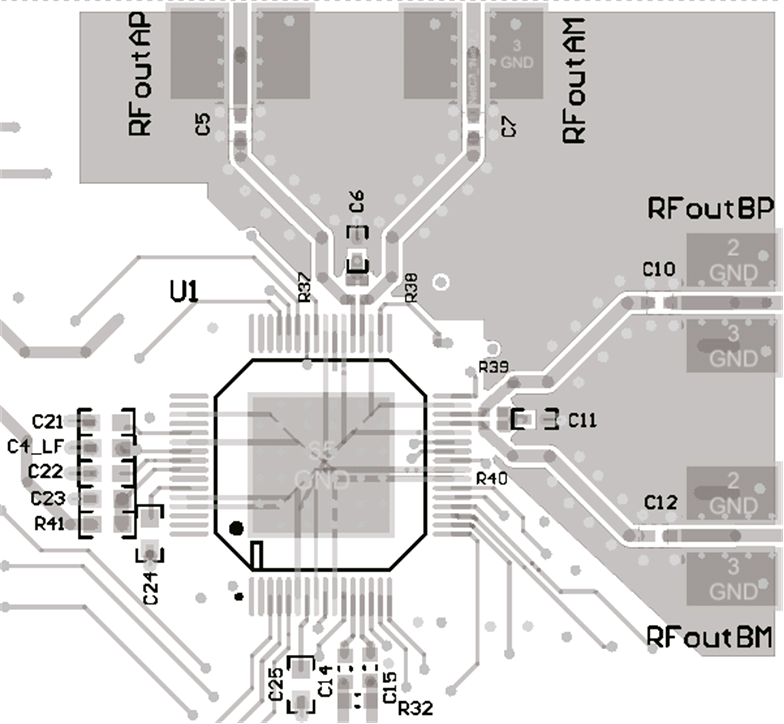
In addition to the layout guidelines already given, here are some additional comments for this specific layout example
- The most critical part of the layout that the placement of the pull-up components (R37, R38, R39, and R40) is close to the pin for optimal output power.
- For this layout, most of the loop filter (C1_LF, C2_LF, C3_LF, R2_LF, R3_LF, and R4_LF) are on the back side of the board. However note that C4_LF is on the top side right next to the Vtune pin. In the event that this C4_LF capacitor would be open, it is recommended to move one of loop capacitors in this spot. For instance, if a 3rd order loop filter was used, technically C3_LF would be non-zero and C4_LF would be open. However, for this layout example that is designed for a 4th order loop filter, it would be optimal to make R3_LF = 0 ohm, C3_LF = open, and C4_LF to be whatever C3_LF would have been.
 Figure 79. LMX2615 Layout Example