ZHCSIC4C
June 2018 – November 2018
LMX2615-SP
PRODUCTION DATA.
1
特性
2
应用
3
说明
Device Images
简化原理图
4
修订历史记录
5
Pin Configuration and Functions
Pin Functions
CQFP Package (QFN) Pin Functions
6
Specifications
6.1
Absolute Maximum Ratings
6.2
ESD Ratings
6.3
Recommended Operating Conditions
6.4
Thermal Information
6.5
Electrical Characteristics
6.6
Timing Requirements
6.7
Typical Characteristics
7
Detailed Description
7.1
Overview
7.2
Functional Block Diagram
7.3
Feature Description
7.3.1
Reference Oscillator Input
7.3.2
Reference Path
7.3.2.1
OSCin Doubler (OSC_2X)
7.3.2.2
Pre-R Divider (PLL_R_PRE)
7.3.2.3
Post-R Divider (PLL_R)
7.3.3
State Machine Clock
7.3.4
PLL Phase Detector and Charge Pump
7.3.5
N Divider and Fractional Circuitry
7.3.6
MUXout Pin
7.3.6.1
Serial data output for readback
7.3.6.2
Lock detect indicator set as type “VCOCal”
7.3.6.3
Lock detect indicator set as type “Vtune and VCOCal”
7.3.7
VCO (Voltage Controlled Oscillator)
7.3.7.1
VCO Calibration
7.3.7.2
Watchdog Feature
7.3.7.3
RECAL Feature
7.3.7.4
Determining the VCO Gain
7.3.8
Channel Divider
7.3.9
Output Buffer
7.3.10
Powerdown Modes
7.3.11
Treatment of Unused Pins
7.3.12
Phase Synchronization
7.3.12.1
General Concept
7.3.12.2
Categories of Applications for SYNC
7.3.12.3
Procedure for Using SYNC
7.3.12.4
SYNC Input Pin
7.3.13
Phase Adjust
7.3.14
Fine Adjustments for Phase Adjust and Phase SYNC
7.3.15
SYSREF
7.3.15.1
Programmable Fields
7.3.15.2
Input and Output Pin Formats
7.3.15.2.1
SYSREF Output Format
7.3.15.3
Examples
7.3.15.4
SYSREF Procedure
7.3.16
Pin Modes
7.4
Device Functional Modes
7.5
Programming
7.5.1
Recommended Initial Power-Up Sequence
7.5.2
Recommended Sequence for Changing Frequencies
7.6
Register Maps
7.6.1
Register Map
7.6.1.1
R0 Register (Address = 0x0) [reset = X]
Table 22.
R0 Register Field Descriptions
7.6.1.2
R1 Register (Address = 0x1) [reset = 0x4]
Table 23.
R1 Register Field Descriptions
7.6.1.3
R8 Register (Address = 0x8) [reset = X]
Table 24.
R8 Register Field Descriptions
7.6.1.4
R9 Register (Address = 0x9) [reset = X]
Table 25.
R9 Register Field Descriptions
7.6.1.5
R11 Register (Address = 0xB) [reset = 0x10]
Table 26.
R11 Register Field Descriptions
7.6.1.6
R12 Register (Address = 0xC) [reset = 0x1]
Table 27.
R12 Register Field Descriptions
7.6.1.7
R14 Register (Address = 0xE) [reset = 0x70]
Table 28.
R14 Register Field Descriptions
7.6.1.8
R16 Register (Address = 0x10) [reset = 0x80]
Table 29.
R16 Register Field Descriptions
7.6.1.9
R19 Register (Address = 0x13) [reset = 0xB7]
Table 30.
R19 Register Field Descriptions
7.6.1.10
R20 Register (Address = 0x14) [reset = X]
Table 31.
R20 Register Field Descriptions
7.6.1.11
R31 Register (Address = 0x1F) [reset = X]
Table 32.
R31 Register Field Descriptions
7.6.1.12
R34 Register (Address = 0x22) [reset = 0x0]
Table 33.
R34 Register Field Descriptions
7.6.1.13
R36 Register (Address = 0x24) [reset = 0x46]
Table 34.
R36 Register Field Descriptions
7.6.1.14
R37 Register (Address = 0x25) [reset = 0x400]
Table 35.
R37 Register Field Descriptions
7.6.1.15
R38 Register (Address = 0x26) [reset = 0xFD51]
Table 36.
R38 Register Field Descriptions
7.6.1.16
R39 Register (Address = 0x27) [reset = 0xDA80]
Table 37.
R39 Register Field Descriptions
7.6.1.17
R40 Register (Address = 0x28) [reset = 0x0]
Table 38.
R40 Register Field Descriptions
7.6.1.18
R41 Register (Address = 0x29) [reset = 0x0]
Table 39.
R41 Register Field Descriptions
7.6.1.19
R42 Register (Address = 0x2A) [reset = 0x0]
Table 40.
R42 Register Field Descriptions
7.6.1.20
R43 Register (Address = 0x2B) [reset = 0x0]
Table 41.
R43 Register Field Descriptions
7.6.1.21
R44 Register (Address = 0x2C) [reset = 0x1FA3]
Table 42.
R44 Register Field Descriptions
7.6.1.22
R45 Register (Address = 0x2D) [reset = X]
Table 43.
R45 Register Field Descriptions
7.6.1.23
R46 Register (Address = 0x2E) [reset = 0x1]
Table 44.
R46 Register Field Descriptions
7.6.1.24
R58 Register (Address = 0x3A) [reset = X]
Table 45.
R58 Register Field Descriptions
7.6.1.25
R59 Register (Address = 0x3B) [reset = 0x1]
Table 46.
R59 Register Field Descriptions
7.6.1.26
R60 Register (Address = 0x3C) [reset = 0x9C4]
Table 47.
R60 Register Field Descriptions
7.6.1.27
R69 Register (Address = 0x45) [reset = 0x0]
Table 48.
R69 Register Field Descriptions
7.6.1.28
R70 Register (Address = 0x46) [reset = 0xC350]
Table 49.
R70 Register Field Descriptions
7.6.1.29
R71 Register (Address = 0x47) [reset = 0x80]
Table 50.
R71 Register Field Descriptions
7.6.1.30
R72 Register (Address = 0x48) [reset = 0x1]
Table 51.
R72 Register Field Descriptions
7.6.1.31
R73 Register (Address = 0x49) [reset = 0x3F]
Table 52.
R73 Register Field Descriptions
7.6.1.32
R74 Register (Address = 0x4A) [reset = 0x0]
Table 53.
R74 Register Field Descriptions
7.6.1.33
R75 Register (Address = 0x4B) [reset = 0x0]
Table 54.
R75 Register Field Descriptions
7.6.1.34
R110 Register (Address = 0x6E) [reset = 0x0]
Table 55.
R110 Register Field Descriptions
7.6.1.35
R111 Register (Address = 0x6F) [reset = 0x0]
Table 56.
R111 Register Field Descriptions
7.6.1.36
R112 Register (Address = 0x70) [reset = 0x0]
Table 57.
R112 Register Field Descriptions
7.6.1.37
R113 Register (Address = 0x71) [reset = 0x0]
Table 58.
R113 Register Field Descriptions
7.6.1.38
R114 Register (Address = 0x72) [reset = 0x26F]
Table 59.
R114 Register Field Descriptions
8
Application and Implementation
8.1
Application Information
8.1.1
OSCin Configuration
8.1.2
OSCin Slew Rate
8.1.3
RF Output Buffer Power Control
8.1.4
RF Output Buffer Pullup
8.1.4.1
Resistor Pullup
8.1.4.2
Inductor Pullup
8.1.4.3
Combination Pullup
8.1.5
RF Output Treatment for the Complimentary Side
8.1.5.1
Single-Ended Termination of Unused Output
8.1.5.2
Differential Termination
8.2
Typical Application
8.2.1
Design Requirements
8.2.2
Detailed Design Procedure
8.2.3
Application Curve
9
Power Supply Recommendations
10
Layout
10.1
Layout Guidelines
10.2
Layout Example
10.3
Footprint Example on PCB Layout
10.4
Radiation Environments
10.4.1
Total Ionizing Dose
10.4.2
Single Event Effect
11
器件和文档支持
11.1
器件支持
11.1.1
第三方米6体育平台手机版_好二三四免责声明
11.1.2
开发支持
11.2
文档支持
11.2.1
相关文档
11.3
商标
11.4
静电放电警告
11.5
术语表
12
机械、封装和可订购信息
12.1
工程样片
12.2
封装机械信息
封装选项
机械数据 (封装 | 引脚)
HBD|64
MCSF001
散热焊盘机械数据 (封装 | 引脚)
订购信息
zhcsic4c_oa
zhcsic4c_pm
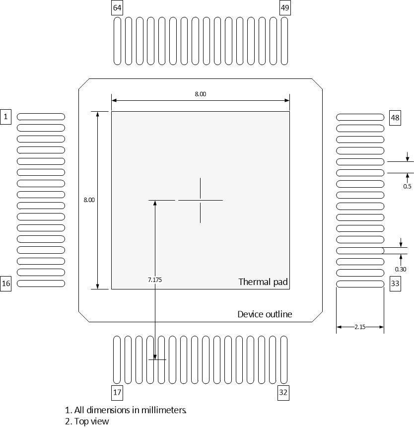
10.3
Footprint Example on PCB Layout
Figure 80.
LMX2615 PCB Layout
千亿体育app官网登录(中国)官方网站IOS/安卓通用版/手机APP
|
米乐app下载官网(中国)|ios|Android/通用版APP最新版
|
米乐|米乐·M6(中国大陆)官方网站
|
千亿体育登陆地址
|
华体会体育(中国)HTH·官方网站
|
千赢qy国际_全站最新版千赢qy国际V6.2.14安卓/IOS下载
|
18新利网v1.2.5|中国官方网站
|
bob电竞真人(中国官网)安卓/ios苹果/电脑版【1.97.95版下载】
|
千亿体育app官方下载(中国)官方网站IOS/安卓/手机APP下载安装
|