ZHCSIC4C June   2018  – November 2018 LMX2615-SP

PRODUCTION DATA.  

  1. 特性
  2. 应用
  3. 说明
    1.     Device Images
      1.      简化原理图
  4. 修订历史记录
  5. Pin Configuration and Functions
    1.     Pin Functions
      1.      CQFP Package (QFN) Pin Functions
  6. Specifications
    1. 6.1 Absolute Maximum Ratings
    2. 6.2 ESD Ratings
    3. 6.3 Recommended Operating Conditions
    4. 6.4 Thermal Information
    5. 6.5 Electrical Characteristics
    6. 6.6 Timing Requirements
    7. 6.7 Typical Characteristics
  7. Detailed Description
    1. 7.1 Overview
    2. 7.2 Functional Block Diagram
    3. 7.3 Feature Description
      1. 7.3.1  Reference Oscillator Input
      2. 7.3.2  Reference Path
        1. 7.3.2.1 OSCin Doubler (OSC_2X)
        2. 7.3.2.2 Pre-R Divider (PLL_R_PRE)
        3. 7.3.2.3 Post-R Divider (PLL_R)
      3. 7.3.3  State Machine Clock
      4. 7.3.4  PLL Phase Detector and Charge Pump
      5. 7.3.5  N Divider and Fractional Circuitry
      6. 7.3.6  MUXout Pin
        1. 7.3.6.1 Serial data output for readback
        2. 7.3.6.2 Lock detect indicator set as type “VCOCal”
        3. 7.3.6.3 Lock detect indicator set as type “Vtune and VCOCal”
      7. 7.3.7  VCO (Voltage Controlled Oscillator)
        1. 7.3.7.1 VCO Calibration
        2. 7.3.7.2 Watchdog Feature
        3. 7.3.7.3 RECAL Feature
        4. 7.3.7.4 Determining the VCO Gain
      8. 7.3.8  Channel Divider
      9. 7.3.9  Output Buffer
      10. 7.3.10 Powerdown Modes
      11. 7.3.11 Treatment of Unused Pins
      12. 7.3.12 Phase Synchronization
        1. 7.3.12.1 General Concept
        2. 7.3.12.2 Categories of Applications for SYNC
        3. 7.3.12.3 Procedure for Using SYNC
        4. 7.3.12.4 SYNC Input Pin
      13. 7.3.13 Phase Adjust
      14. 7.3.14 Fine Adjustments for Phase Adjust and Phase SYNC
      15. 7.3.15 SYSREF
        1. 7.3.15.1 Programmable Fields
        2. 7.3.15.2 Input and Output Pin Formats
          1. 7.3.15.2.1 SYSREF Output Format
        3. 7.3.15.3 Examples
        4. 7.3.15.4 SYSREF Procedure
      16. 7.3.16 Pin Modes
    4. 7.4 Device Functional Modes
    5. 7.5 Programming
      1. 7.5.1 Recommended Initial Power-Up Sequence
      2. 7.5.2 Recommended Sequence for Changing Frequencies
    6. 7.6 Register Maps
      1. 7.6.1 Register Map
        1. 7.6.1.1  R0 Register (Address = 0x0) [reset = X]
          1. Table 22. R0 Register Field Descriptions
        2. 7.6.1.2  R1 Register (Address = 0x1) [reset = 0x4]
          1. Table 23. R1 Register Field Descriptions
        3. 7.6.1.3  R8 Register (Address = 0x8) [reset = X]
          1. Table 24. R8 Register Field Descriptions
        4. 7.6.1.4  R9 Register (Address = 0x9) [reset = X]
          1. Table 25. R9 Register Field Descriptions
        5. 7.6.1.5  R11 Register (Address = 0xB) [reset = 0x10]
          1. Table 26. R11 Register Field Descriptions
        6. 7.6.1.6  R12 Register (Address = 0xC) [reset = 0x1]
          1. Table 27. R12 Register Field Descriptions
        7. 7.6.1.7  R14 Register (Address = 0xE) [reset = 0x70]
          1. Table 28. R14 Register Field Descriptions
        8. 7.6.1.8  R16 Register (Address = 0x10) [reset = 0x80]
          1. Table 29. R16 Register Field Descriptions
        9. 7.6.1.9  R19 Register (Address = 0x13) [reset = 0xB7]
          1. Table 30. R19 Register Field Descriptions
        10. 7.6.1.10 R20 Register (Address = 0x14) [reset = X]
          1. Table 31. R20 Register Field Descriptions
        11. 7.6.1.11 R31 Register (Address = 0x1F) [reset = X]
          1. Table 32. R31 Register Field Descriptions
        12. 7.6.1.12 R34 Register (Address = 0x22) [reset = 0x0]
          1. Table 33. R34 Register Field Descriptions
        13. 7.6.1.13 R36 Register (Address = 0x24) [reset = 0x46]
          1. Table 34. R36 Register Field Descriptions
        14. 7.6.1.14 R37 Register (Address = 0x25) [reset = 0x400]
          1. Table 35. R37 Register Field Descriptions
        15. 7.6.1.15 R38 Register (Address = 0x26) [reset = 0xFD51]
          1. Table 36. R38 Register Field Descriptions
        16. 7.6.1.16 R39 Register (Address = 0x27) [reset = 0xDA80]
          1. Table 37. R39 Register Field Descriptions
        17. 7.6.1.17 R40 Register (Address = 0x28) [reset = 0x0]
          1. Table 38. R40 Register Field Descriptions
        18. 7.6.1.18 R41 Register (Address = 0x29) [reset = 0x0]
          1. Table 39. R41 Register Field Descriptions
        19. 7.6.1.19 R42 Register (Address = 0x2A) [reset = 0x0]
          1. Table 40. R42 Register Field Descriptions
        20. 7.6.1.20 R43 Register (Address = 0x2B) [reset = 0x0]
          1. Table 41. R43 Register Field Descriptions
        21. 7.6.1.21 R44 Register (Address = 0x2C) [reset = 0x1FA3]
          1. Table 42. R44 Register Field Descriptions
        22. 7.6.1.22 R45 Register (Address = 0x2D) [reset = X]
          1. Table 43. R45 Register Field Descriptions
        23. 7.6.1.23 R46 Register (Address = 0x2E) [reset = 0x1]
          1. Table 44. R46 Register Field Descriptions
        24. 7.6.1.24 R58 Register (Address = 0x3A) [reset = X]
          1. Table 45. R58 Register Field Descriptions
        25. 7.6.1.25 R59 Register (Address = 0x3B) [reset = 0x1]
          1. Table 46. R59 Register Field Descriptions
        26. 7.6.1.26 R60 Register (Address = 0x3C) [reset = 0x9C4]
          1. Table 47. R60 Register Field Descriptions
        27. 7.6.1.27 R69 Register (Address = 0x45) [reset = 0x0]
          1. Table 48. R69 Register Field Descriptions
        28. 7.6.1.28 R70 Register (Address = 0x46) [reset = 0xC350]
          1. Table 49. R70 Register Field Descriptions
        29. 7.6.1.29 R71 Register (Address = 0x47) [reset = 0x80]
          1. Table 50. R71 Register Field Descriptions
        30. 7.6.1.30 R72 Register (Address = 0x48) [reset = 0x1]
          1. Table 51. R72 Register Field Descriptions
        31. 7.6.1.31 R73 Register (Address = 0x49) [reset = 0x3F]
          1. Table 52. R73 Register Field Descriptions
        32. 7.6.1.32 R74 Register (Address = 0x4A) [reset = 0x0]
          1. Table 53. R74 Register Field Descriptions
        33. 7.6.1.33 R75 Register (Address = 0x4B) [reset = 0x0]
          1. Table 54. R75 Register Field Descriptions
        34. 7.6.1.34 R110 Register (Address = 0x6E) [reset = 0x0]
          1. Table 55. R110 Register Field Descriptions
        35. 7.6.1.35 R111 Register (Address = 0x6F) [reset = 0x0]
          1. Table 56. R111 Register Field Descriptions
        36. 7.6.1.36 R112 Register (Address = 0x70) [reset = 0x0]
          1. Table 57. R112 Register Field Descriptions
        37. 7.6.1.37 R113 Register (Address = 0x71) [reset = 0x0]
          1. Table 58. R113 Register Field Descriptions
        38. 7.6.1.38 R114 Register (Address = 0x72) [reset = 0x26F]
          1. Table 59. R114 Register Field Descriptions
  8. Application and Implementation
    1. 8.1 Application Information
      1. 8.1.1 OSCin Configuration
      2. 8.1.2 OSCin Slew Rate
      3. 8.1.3 RF Output Buffer Power Control
      4. 8.1.4 RF Output Buffer Pullup
        1. 8.1.4.1 Resistor Pullup
        2. 8.1.4.2 Inductor Pullup
        3. 8.1.4.3 Combination Pullup
      5. 8.1.5 RF Output Treatment for the Complimentary Side
        1. 8.1.5.1 Single-Ended Termination of Unused Output
        2. 8.1.5.2 Differential Termination
    2. 8.2 Typical Application
      1. 8.2.1 Design Requirements
      2. 8.2.2 Detailed Design Procedure
      3. 8.2.3 Application Curve
  9. Power Supply Recommendations
  10. 10Layout
    1. 10.1 Layout Guidelines
    2. 10.2 Layout Example
    3. 10.3 Footprint Example on PCB Layout
    4. 10.4 Radiation Environments
      1. 10.4.1 Total Ionizing Dose
      2. 10.4.2 Single Event Effect
  11. 11器件和文档支持
    1. 11.1 器件支持
      1. 11.1.1 第三方米6体育平台手机版_好二三四免责声明
      2. 11.1.2 开发支持
    2. 11.2 文档支持
      1. 11.2.1 相关文档
    3. 11.3 商标
    4. 11.4 静电放电警告
    5. 11.5 术语表
  12. 12机械、封装和可订购信息
    1. 12.1 工程样片
    2. 12.2 封装机械信息

封装选项

机械数据 (封装 | 引脚)
散热焊盘机械数据 (封装 | 引脚)
订购信息

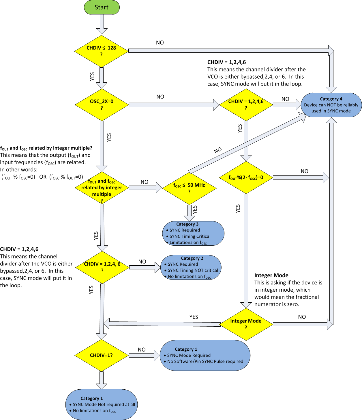
Categories of Applications for SYNC

The requirements for SYNC depend on certain setup conditions. In cases that the SYNC is not timing critical, it can be done through software by toggling the VCO_PHASE_SYNC bit from 0 to 1. The Figure 26 gives the different categories. When it is timing critical, then it must be done through the pin and the setup and hold times for the OSCin pin are critical. For timing critical sync (Category 3) ONLY, adhere to the following guidelines.

Table 13. SYNC Pin Timing Characteristics for Category 3 SYNC

Parameter Description Min Max Unit
fOSC Input reference Frequency 40 MHz
tSETUP Setup time between SYNC and OSCin rising edges 2.5 ns
tHOLD Hold time between SYNC and OSCin rising edges 2.5 ns
LMX2615-SP flow-chrt-01-snas736.gifFigure 26. Determining the SYNC Category