ZHCS546P December 2009 – April 2019 LMZ10504
PRODUCTION DATA.
- 1 特性
- 2 应用
- 3 说明
- 4 修订历史记录
- 5 Pin Configuration and Functions
- 6 Specifications
- 7 Detailed Description
- 8 Application and Implementation
- 9 Power Supply Recommendations
- 10Layout
- 11器件和文档支持
- 12机械、封装和可订购信息
10.4 Power Module SMT Guidelines
The recommendations below are for a standard module surface mount assembly.
- Land Pattern – Follow the PCB land pattern with either soldermask defined or non-soldermask defined pads
- Stencil Aperture
- For the exposed die attach pad (DAP), adjust the stencil for approximately 80% coverage of the PCB land pattern
- For all other I/O pads use a 1:1 ratio between the aperture and the land pattern recommendation
- Solder Paste – Use a standard SAC Alloy such as SAC 305, type 3 or higher
- Stencil Thickness – 0.125 to 0.15 mm
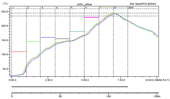
- Reflow - Refer to solder paste supplier recommendation and optimized per board size and density
- Maximum number of reflows allowed is one
- Refer to Design Summary LMZ1xxx and LMZ2xxx Power Modules Family (SNAA214) for reflow information.
 Figure 35. Sample Reflow Profile
 Table 11. Sample Reflow Profile Table
| PROBE | MAX TEMP (°C) | REACHED MAX TEMP | TIME ABOVE 235°C | REACHED 235°C | TIME ABOVE 245°C | REACHED 245°C | TIME ABOVE 260°C | REACHED 260°C |
|---|---|---|---|---|---|---|---|---|
| 1 | 242.5 | 6.58 | 0.49 | 6.39 | 0.00 | – | 0.00 | – |
| 2 | 242.5 | 7.10 | 0.55 | 6.31 | 0.00 | 7.10 | 0.00 | – |
| 3 | 241.0 | 7.09 | 0.42 | 6.44 | 0.00 | – | 0.00 | – |