ZHCSD73D August   2012  – August 2018 LMZ21700

PRODUCTION DATA.  

  1. 特性
  2. 应用
  3. 说明
    1.     Device Images
      1.      简化原理图
      2.      VIN = 12V 时的效率
  4. 修订历史记录
  5. Pin Configuration and Functions
    1. Table 1. Pin Functions
  6. Specifications
    1. 6.1 Absolute Maximum Ratings
    2. 6.2 Handling Ratings
    3. 6.3 Recommended Operating Conditions
    4. 6.4 Thermal Information
    5. 6.5 Electrical Characteristics
    6. 6.6 Typical Characteristics
  7. Detailed Description
    1. 7.1 Overview
    2. 7.2 Functional Block Diagram
    3. 7.3 Package Construction
    4. 7.4 Feature Description
      1. 7.4.1 Input Under Voltage Lockout
      2. 7.4.2 Enable Input (EN)
      3. 7.4.3 Softstart and Tracking Function (SS)
      4. 7.4.4 Power Good Function (PG)
      5. 7.4.5 Output Voltage Setting
      6. 7.4.6 Output Current Limit and Output Short Circuit Protection
      7. 7.4.7 Thermal Protection
    5. 7.5 Device Functional Modes
      1. 7.5.1 PWM Mode Operation
      2. 7.5.2 PSM Operation
  8. Application and Implementation
    1. 8.1 Application Information
    2. 8.2 Typical Application
      1. 8.2.1 Design Requirements
      2. 8.2.2 Detailed Design Procedure
        1. 8.2.2.1 Input Capacitor (CIN)
        2. 8.2.2.2 Output Capacitor (COUT)
        3. 8.2.2.3 Softstart Capacitor (CSS)
        4. 8.2.2.4 Power Good Resistor (RPG)
        5. 8.2.2.5 Feedback Resistors (RFBB and RFBT)
      3. 8.2.3 Application Curves
        1. 8.2.3.1 VOUT = 1.2 V
        2. 8.2.3.2 VOUT = 1.8 V
        3. 8.2.3.3 VOUT = 2.5 V
        4. 8.2.3.4 VOUT = 3.3 V
        5. 8.2.3.5 VOUT = 5.0 V
    3. 8.3 Do's and Don'ts
  9. Power Supply Recommendations
    1. 9.1 Voltage Range
    2. 9.2 Current Capability
    3. 9.3 Input Connection
      1. 9.3.1 Voltage Drops
      2. 9.3.2 Stability
  10. 10Layout
    1. 10.1 Layout Guidelines
      1. 10.1.1 Minimize the High di/dt Loop Area
      2. 10.1.2 Protect the Sensitive Nodes in the Circuit
      3. 10.1.3 Provide Thermal Path and Shielding
    2. 10.2 Layout Example
      1. 10.2.1 High Density Layout Example for Space Constrained Applications
        1. 10.2.1.1 35 mm² Solution Size (Single Sided)
  11. 11器件和文档支持
    1. 11.1 器件支持
    2. 11.2 开发支持
      1. 11.2.1 使用 WEBENCH® 工具创建定制设计
    3. 11.3 接收文档更新通知
    4. 11.4 社区资源
    5. 11.5 商标
    6. 11.6 静电放电警告
    7. 11.7 术语表
  12. 12机械、封装和可订购信息
    1. 12.1 Tape and Reel Information

封装选项

请参考 PDF 数据表获取器件具体的封装图。

机械数据 (封装 | 引脚)
  • SIL|8
散热焊盘机械数据 (封装 | 引脚)
订购信息

VOUT = 2.5 V

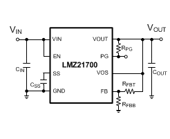
LMZ21700 TYP_SCH_00.gifFigure 44. Typical Applications Circuit
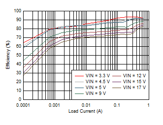
LMZ21700 D017_LMZ21700_25C_2.5VOUT_EFFICIENCY_LOG_SNVS872.gifFigure 46. Efficiency VOUT = 2.5 V
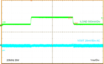
LMZ21700 LMZ21700_2.5VOUT_LOAD_TRANS_100mA_to_650mA_snvs872.gifFigure 48. Load Transient VOUT = 2.5 V
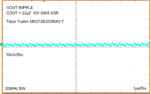
LMZ21700 LMZ21700_2.5VOUT_RIPPLE_20MHzBW_snvs872.gifFigure 50. 20MHz Oscilloscope Bandwidth
Output Voltage Ripple VOUT = 2.5 V
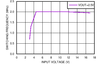
LMZ21700 LMZ21700_FSW_2.5VOUT_snvs872.pngFigure 52. Typical Switching Frequency at 650mA Load VOUT = 2.5 V
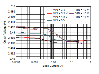
LMZ21700 D018_LMZ21700_25C_2.5VOUT_LINE_AND_LOAD_REG_LOG_SNVS872.gifFigure 54. Line and Load Regulation VOUT = 2.5 V
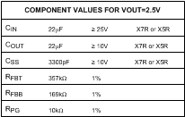
LMZ21700 2.5V_BOM_snvs872.gifFigure 45. External Component Values
(VOUT = 2.5 V)
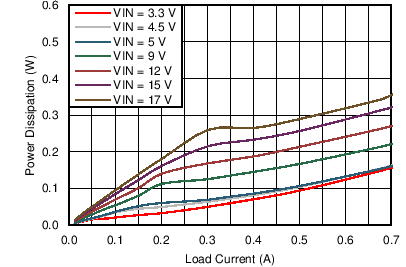
LMZ21700 LMZ21700_25C_2.5VOUT_POWER_DISSIPATION_snvs872.pngFigure 47. Power Dissipation VOUT = 2.5 V
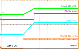
LMZ21700 LMZ21700_2.5VOUT_STARTUP_snvs872.gifFigure 49. Startup VOUT = 2.5 V
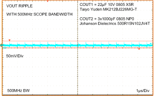
LMZ21700 LMZ21700_2.5VOUT_RIPPLE_500MHzBW_snvs872.gifFigure 51. 500MHz Oscilloscope Bandwidth, 3x1000pF additional output capacitance
Output Voltage Ripple and HF Noise VOUT = 2.5 V
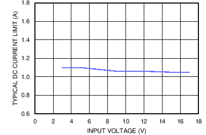
LMZ21700 LMZ21700_ICL_2.5V_85C_snvs872.pngFigure 53. Typical Current Limit VOUT = 2.5 V, TA = 85 °C
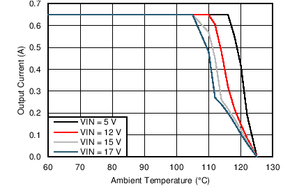
LMZ21700 LMZ21700SIL_2.5VO_47CperW_snvs872.pngFigure 55. Thermal Derating for θJA=47ºC/W, VOUT = 2.5 V