ZHCSD73D August   2012  – August 2018 LMZ21700

PRODUCTION DATA.  

  1. 特性
  2. 应用
  3. 说明
    1.     Device Images
      1.      简化原理图
      2.      VIN = 12V 时的效率
  4. 修订历史记录
  5. Pin Configuration and Functions
    1. Table 1. Pin Functions
  6. Specifications
    1. 6.1 Absolute Maximum Ratings
    2. 6.2 Handling Ratings
    3. 6.3 Recommended Operating Conditions
    4. 6.4 Thermal Information
    5. 6.5 Electrical Characteristics
    6. 6.6 Typical Characteristics
  7. Detailed Description
    1. 7.1 Overview
    2. 7.2 Functional Block Diagram
    3. 7.3 Package Construction
    4. 7.4 Feature Description
      1. 7.4.1 Input Under Voltage Lockout
      2. 7.4.2 Enable Input (EN)
      3. 7.4.3 Softstart and Tracking Function (SS)
      4. 7.4.4 Power Good Function (PG)
      5. 7.4.5 Output Voltage Setting
      6. 7.4.6 Output Current Limit and Output Short Circuit Protection
      7. 7.4.7 Thermal Protection
    5. 7.5 Device Functional Modes
      1. 7.5.1 PWM Mode Operation
      2. 7.5.2 PSM Operation
  8. Application and Implementation
    1. 8.1 Application Information
    2. 8.2 Typical Application
      1. 8.2.1 Design Requirements
      2. 8.2.2 Detailed Design Procedure
        1. 8.2.2.1 Input Capacitor (CIN)
        2. 8.2.2.2 Output Capacitor (COUT)
        3. 8.2.2.3 Softstart Capacitor (CSS)
        4. 8.2.2.4 Power Good Resistor (RPG)
        5. 8.2.2.5 Feedback Resistors (RFBB and RFBT)
      3. 8.2.3 Application Curves
        1. 8.2.3.1 VOUT = 1.2 V
        2. 8.2.3.2 VOUT = 1.8 V
        3. 8.2.3.3 VOUT = 2.5 V
        4. 8.2.3.4 VOUT = 3.3 V
        5. 8.2.3.5 VOUT = 5.0 V
    3. 8.3 Do's and Don'ts
  9. Power Supply Recommendations
    1. 9.1 Voltage Range
    2. 9.2 Current Capability
    3. 9.3 Input Connection
      1. 9.3.1 Voltage Drops
      2. 9.3.2 Stability
  10. 10Layout
    1. 10.1 Layout Guidelines
      1. 10.1.1 Minimize the High di/dt Loop Area
      2. 10.1.2 Protect the Sensitive Nodes in the Circuit
      3. 10.1.3 Provide Thermal Path and Shielding
    2. 10.2 Layout Example
      1. 10.2.1 High Density Layout Example for Space Constrained Applications
        1. 10.2.1.1 35 mm² Solution Size (Single Sided)
  11. 11器件和文档支持
    1. 11.1 器件支持
    2. 11.2 开发支持
      1. 11.2.1 使用 WEBENCH® 工具创建定制设计
    3. 11.3 接收文档更新通知
    4. 11.4 社区资源
    5. 11.5 商标
    6. 11.6 静电放电警告
    7. 11.7 术语表
  12. 12机械、封装和可订购信息
    1. 12.1 Tape and Reel Information

封装选项

请参考 PDF 数据表获取器件具体的封装图。

机械数据 (封装 | 引脚)
  • SIL|8
散热焊盘机械数据 (封装 | 引脚)
订购信息

Provide Thermal Path and Shielding

Using the available layers in the PCB can help provide additional shielding and improved thermal performance. Large unbroken GND copper areas provide good thermal and return current paths. Flood unused PCB area with GND copper. Use thermal vias to connect the GND copper between layers.

The required board area for proper thermal dissipation can be estimated using the power dissipation curves for the desired output voltage and the package thermal resistance vs. board area curve. Refer to the power dissipation graphs in the Typical Characteristics section. Using the power dissipation (PDISS) for the designed input and output voltage and the max operating ambient temperature TA for the application, estimate the required thermal resistance RθJA with the following expression.

Equation 8. RθJA - REQUIRED≤ (125 ºC - TA) / PDISS

Then use Figure 80 to estimate the board copper area required to achieve the calculated thermal resistance.
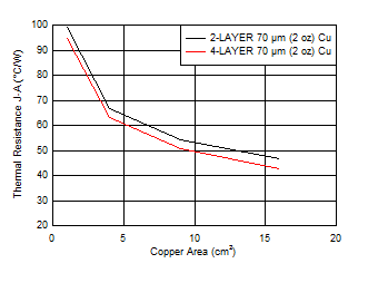
LMZ21700 D012_LMZ21700_PACKAGE_THERMAL_VS_PCB_SNVS872.gifFigure 80. Package Thermal Resistance vs. Board Copper Area, No Air Flow

For example, for a design with 17 V input and 5 V output and 0.65 A load the power dissipation according to Figure 7 is 0.43 W.

For 85 °C ambient temperature, the RθJA-REQUIRED is ≤ (125 °C - 85 °C) / 0.43 W, or ≤ 93 °C/W. Looking at Figure 80 the minimum copper area required to achieve this thermal resistance with a 4-layer board and 70 µm (2 oz) copper is approximately 1 cm².