ZHCS809E June 2013 – February 2020 LMZ31707
PRODUCTION DATA.
- 1 特性
- 2 应用
- 3 说明
- 4 修订历史记录
- 5 Specifications
- 6 Device Information
- 7 Typical Characteristics (PVIN = VIN = 12 V)
- 8 Typical Characteristics (PVIN = VIN = 5 V)
- 9 Typical Characteristics (PVIN = 3.3 V, VIN = 5 V)
-
10Application Information
- 10.1 Adjusting the Output Voltage
- 10.2 Capacitor Recommendations for the LMZ31707 Power Supply
- 10.3 Transient Response
- 10.4 Transient Waveforms
- 10.5 Application Schematics
- 10.6 Custom Design With WEBENCH® Tools
- 10.7 VIN and PVIN Input Voltage
- 10.8 3.3 V PVIN Operation
- 10.9 Power Good (PWRGD)
- 10.10 SYNC_OUT
- 10.11 Parallel Operation
- 10.12 Light Load Efficiency (LLE)
- 10.13 Power-Up Characteristics
- 10.14 Pre-Biased Start-up
- 10.15 Remote Sense
- 10.16 Thermal Shutdown
- 10.17 Output On/Off Inhibit (INH)
- 10.18 Slow Start (SS/TR)
- 10.19 Overcurrent Protection
- 10.20 Synchronization (CLK)
- 10.21 Sequencing (SS/TR)
- 10.22 Programmable Undervoltage Lockout (UVLO)
- 10.23 Layout Considerations
- 10.24 EMI
- 11器件和文档支持
- 12机械、封装和可订购信息
10.21 Sequencing (SS/TR)
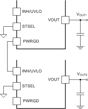
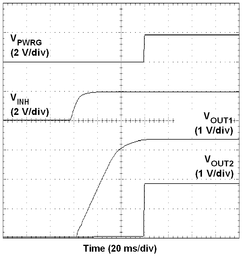
Many of the common power supply sequencing methods can be implemented using the SS/TR, INH and PWRGD pins. The sequential method is illustrated in Figure 35 using two LMZ31707 devices. The PWRGD pin of the first device is coupled to the INH pin of the second device which enables the second power supply once the primary supply reaches regulation. Figure 36 shows sequential turnon waveforms of two LMZ31707 devices.
 Figure 35. Sequencing Schematic
  Figure 36. Sequencing Waveforms
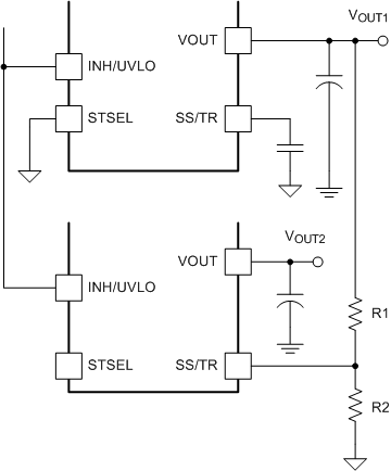
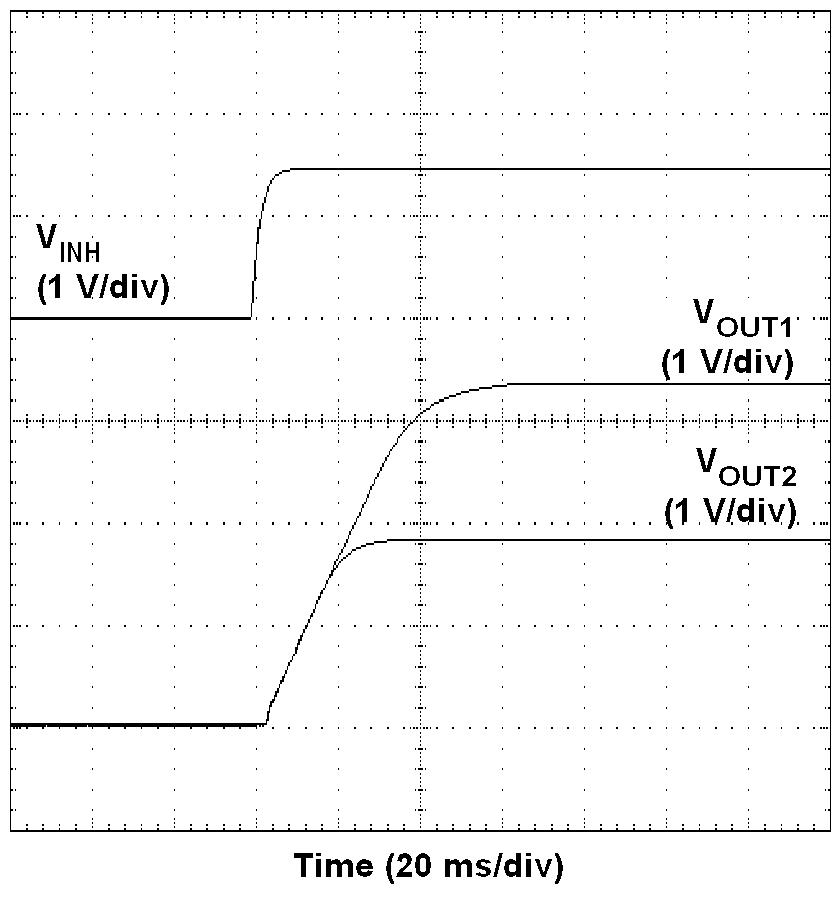
 Simultaneous power supply sequencing can be implemented by connecting the resistor network of R1 and R2 shown in Figure 37 to the output of the power supply that needs to be tracked or to another voltage reference source. The tracking voltage must exceed 750 mV before VOUT2 reaches its set-point voltage. The PWRGD output of the VOUT2 device can remain low if the tracking voltage does not exceed 1.4 V.Figure 38 shows simultaneous turnon waveforms of two LMZ31707 devices. Use and to calculate the values of R1 and R2.
 Figure 37. Simultaneous Tracking Schematic
  Figure 38. Simultaneous Tracking Waveforms