ZHCSBC7E JULY 2013 – December 2019 LMZ31710
PRODUCTION DATA.
- 1 特性
- 2 应用
- 3 说明
- 4 修订历史记录
- 5 Pin Configuration and Functions
- 6 Specifications
-
7 Detailed Description
- 7.1 Overview
- 7.2 Functional Block Diagram
- 7.3
Feature Description
- 7.3.1 VIN and PVIN Input Voltage
- 7.3.2 3.3-V PVIN Operation
- 7.3.3 Adjusting the Output Voltage (0.6 V to 5.5 V)
- 7.3.4 Capacitor Recommendations For the LMZ31710 Power Supply
- 7.3.5 Transient Response
- 7.3.6 Power Good (PWRGD)
- 7.3.7 Light Load Efficiency (LLE)
- 7.3.8 SYNC_OUT
- 7.3.9 Parallel Operation
- 7.3.10 Power-Up Characteristics
- 7.3.11 Pre-Biased Start-Up
- 7.3.12 Remote Sense
- 7.3.13 Thermal Shutdown
- 7.3.14 Output On/Off Inhibit (INH)
- 7.3.15 Slow Start (SS/TR)
- 7.3.16 Overcurrent Protection
- 7.3.17 Synchronization (CLK)
- 7.3.18 Sequencing (SS/TR)
- 7.4 Device Functional Modes
- 8 Application and Implementation
- 9 Power Supply Recommendations
- 10Layout
- 11器件和文档支持
- 12机械、封装和可订购信息
8.3 Additional Application Schematics
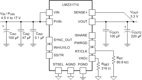
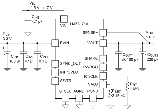
Figure 43 and Figure 44 show additional typical schematics. Figure 43 shows a typical schematic for a 3.3 V output while PVIN and VIN are tied to the same input voltage rail. Figure 44 shows a typical schematic for a 1.0 V output, however PVIN and VIN are powered from separate input voltage rails.
 Figure 43. Typical Schematic
PVIN = VIN = 4.5 V To 17 V, Vout = 3.3 V
 Figure 44. Typical Schematic
PVIN = 3.3 V, VIN = 4.5 V To 17 V, Vout = 1.0 V