ZHCSEU9C March   2016  – June 2018 LMZ34202

PRODUCTION DATA.  

  1. 特性
  2. 应用
  3. 说明
    1.     Device Images
      1.      简化应用
      2.      效率与输出电流间的关系
  4. 修订历史记录
  5. Pin Configuration and Functions
    1.     Pin Functions
  6. Specifications
    1. 6.1 Absolute Maximum Ratings
    2. 6.2 ESD Ratings
    3. 6.3 Recommended Operating Conditions
    4. 6.4 Thermal Information
    5. 6.5 Electrical Characteristics
    6. 6.6 Switching Characteristics
    7. 6.7 Typical Characteristics
    8. 6.8 Typical Characteristics (Thermal Derating)
  7. Detailed Description
    1. 7.1 Overview
    2. 7.2 Functional Block Diagram
    3. 7.3 Feature Description
      1. 7.3.1  Adjusting the Output Voltage
      2. 7.3.2  Switching Frequency (RT)
      3. 7.3.3  Recommended Operating Range
      4. 7.3.4  Synchronization (CLK)
      5. 7.3.5  Output Capacitor Selection
      6. 7.3.6  VERSA-COMP Pin Configurations
      7. 7.3.7  Input Capacitor Selection
      8. 7.3.8  Output On/Off Inhibit (INH/UVLO)
      9. 7.3.9  Under Voltage Lockout (UVLO)
      10. 7.3.10 Remote Sense
      11. 7.3.11 VBSEL
      12. 7.3.12 Soft-Start (SS/TR)
      13. 7.3.13 Power Good (PWRGD) and Pull-up (PWRGD_PU)
      14. 7.3.14 Overcurrent Protection
      15. 7.3.15 Thermal Shutdown
    4. 7.4 Device Functional Modes
      1. 7.4.1 Active Mode
      2. 7.4.2 Light Load Operation
      3. 7.4.3 Shutdown Mode
  8. Application and Implementation
    1. 8.1 Application Information
    2. 8.2 Typical Application
      1. 8.2.1 Minimum External Component Application
        1. 8.2.1.1 Design Requirements
        2. 8.2.1.2 Detailed Design Procedure
          1. 8.2.1.2.1 Custom Design With WEBENCH® Tools
          2. 8.2.1.2.2 Output Voltage Set-Point
          3. 8.2.1.2.3 RT and RTSEL
          4. 8.2.1.2.4 VERSA-COMP
          5. 8.2.1.2.5 VBSEL
          6. 8.2.1.2.6 Input Capacitors
          7. 8.2.1.2.7 Output Capacitors
        3. 8.2.1.3 Application Curves
      2. 8.2.2 INH Control Application
        1. 8.2.2.1 Design Requirements
      3. 8.2.3 Detailed Design Procedure
        1. 8.2.3.1 Switching Frequency
        2. 8.2.3.2 Power Good
        3. 8.2.3.3 Inhibit Control
        4. 8.2.3.4 VERSA-COMP
        5. 8.2.3.5 VBSEL
        6. 8.2.3.6 Soft-Start Capacitors
        7. 8.2.3.7 Input Capacitors
        8. 8.2.3.8 Output Capacitors
  9. Power Supply Recommendations
  10. 10Layout
    1. 10.1 Layout Guidelines
    2. 10.2 Layout Example
    3. 10.3 EMI
  11. 11器件和文档支持
    1. 11.1 器件支持
      1. 11.1.1 开发支持
        1. 11.1.1.1 使用 WEBENCH® 工具创建定制设计
      2. 11.1.2 第三方米6体育平台手机版_好二三四免责声明
    2. 11.2 接收文档更新通知
    3. 11.3 社区资源
    4. 11.4 商标
    5. 11.5 静电放电警告
    6. 11.6 术语表
  12. 12机械、封装和可订购信息

封装选项

机械数据 (封装 | 引脚)
散热焊盘机械数据 (封装 | 引脚)
订购信息

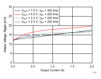
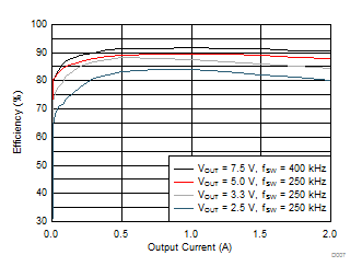
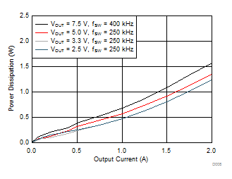
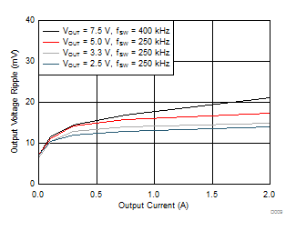
Typical Characteristics

TA = 25°C, unless otherwise noted.
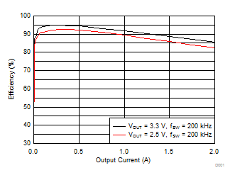
LMZ34202 D001_LMZ36002D5Veff.gif
PVIN = 5 V
Figure 1. Efficiency vs Output Current
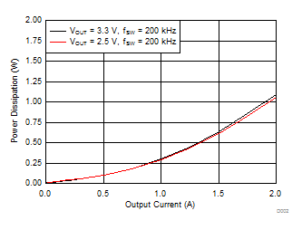
LMZ34202 D002_LMZ36002D5Vpdis.gif
PVIN = 5 V
Figure 3. Power Dissipation vs Output Current
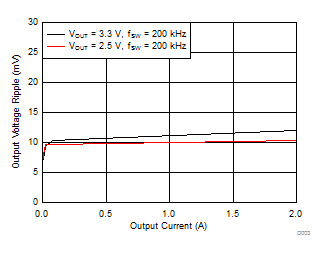
LMZ34202 D003_LMZ36002D5Vrppl.gif
PVIN = 5 V
Figure 5. Voltage Ripple vs Output Current
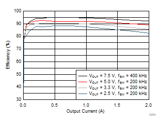
LMZ34202 D004_LMZ36002D12Veff.gif
PVIN = 12 V
Figure 2. Efficiency vs Output Current
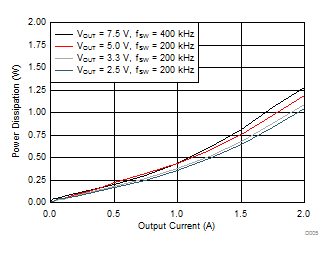
LMZ34202 D007_LMZ36002D12Vpdis2.gif
PVIN = 12 V
Figure 4. Power Dissipation vs Output Current
LMZ34202 D006_LMZ36002D12Vrppl2.gif
PVIN = 12 V
Figure 6. Voltage Ripple vs Output Current
LMZ34202 D007_LMZ36002D24Veff.gif
PVIN = 24 V
Figure 7. Efficiency vs Output Current
LMZ34202 D008_LMZ36002D24Vpdis.gif
PVIN = 24 V
Figure 9. Power Dissipation vs Output Current
LMZ34202 D009_LMZ36002D24Vrppl.gif
PVIN = 24 V
Figure 11. Voltage Ripple vs Output Current
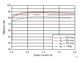
LMZ34202 D010_LMZ36002D24V5Veff.gif
PVIN = 24 V
VOUT = 5 V over frequency range
Figure 8. Efficiency vs Output Current
LMZ34202 D011_LMZ36002D24V5Vpdis.gif
PVIN = 24 V
VOUT = 5 V over frequency range
Figure 10. Power Dissipation vs Output Current
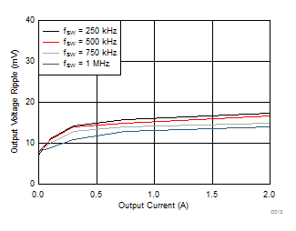
LMZ34202 D012_LMZ36002D24V5Vrppl.gif
PVIN = 24 V
VOUT = 5 V over frequency range
Figure 12. Voltage Ripple vs Output Current
LMZ34202 D013_LMZ36002D36Veff.gif
PVIN = 36V
Figure 13. Efficiency vs Output Current
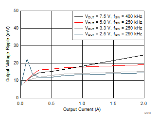
LMZ34202 D015_LMZ36002D36Vrppl.gif
PVIN = 36 V
Figure 15. Voltage Ripple vs Output Current
LMZ34202 D014_LMZ36002D36Vpdis.gif
PVIN = 36 V
Figure 14. Power Dissipation vs Output Current