ZHCSEU9C March   2016  – June 2018 LMZ34202

PRODUCTION DATA.  

  1. 特性
  2. 应用
  3. 说明
    1.     Device Images
      1.      简化应用
      2.      效率与输出电流间的关系
  4. 修订历史记录
  5. Pin Configuration and Functions
    1.     Pin Functions
  6. Specifications
    1. 6.1 Absolute Maximum Ratings
    2. 6.2 ESD Ratings
    3. 6.3 Recommended Operating Conditions
    4. 6.4 Thermal Information
    5. 6.5 Electrical Characteristics
    6. 6.6 Switching Characteristics
    7. 6.7 Typical Characteristics
    8. 6.8 Typical Characteristics (Thermal Derating)
  7. Detailed Description
    1. 7.1 Overview
    2. 7.2 Functional Block Diagram
    3. 7.3 Feature Description
      1. 7.3.1  Adjusting the Output Voltage
      2. 7.3.2  Switching Frequency (RT)
      3. 7.3.3  Recommended Operating Range
      4. 7.3.4  Synchronization (CLK)
      5. 7.3.5  Output Capacitor Selection
      6. 7.3.6  VERSA-COMP Pin Configurations
      7. 7.3.7  Input Capacitor Selection
      8. 7.3.8  Output On/Off Inhibit (INH/UVLO)
      9. 7.3.9  Under Voltage Lockout (UVLO)
      10. 7.3.10 Remote Sense
      11. 7.3.11 VBSEL
      12. 7.3.12 Soft-Start (SS/TR)
      13. 7.3.13 Power Good (PWRGD) and Pull-up (PWRGD_PU)
      14. 7.3.14 Overcurrent Protection
      15. 7.3.15 Thermal Shutdown
    4. 7.4 Device Functional Modes
      1. 7.4.1 Active Mode
      2. 7.4.2 Light Load Operation
      3. 7.4.3 Shutdown Mode
  8. Application and Implementation
    1. 8.1 Application Information
    2. 8.2 Typical Application
      1. 8.2.1 Minimum External Component Application
        1. 8.2.1.1 Design Requirements
        2. 8.2.1.2 Detailed Design Procedure
          1. 8.2.1.2.1 Custom Design With WEBENCH® Tools
          2. 8.2.1.2.2 Output Voltage Set-Point
          3. 8.2.1.2.3 RT and RTSEL
          4. 8.2.1.2.4 VERSA-COMP
          5. 8.2.1.2.5 VBSEL
          6. 8.2.1.2.6 Input Capacitors
          7. 8.2.1.2.7 Output Capacitors
        3. 8.2.1.3 Application Curves
      2. 8.2.2 INH Control Application
        1. 8.2.2.1 Design Requirements
      3. 8.2.3 Detailed Design Procedure
        1. 8.2.3.1 Switching Frequency
        2. 8.2.3.2 Power Good
        3. 8.2.3.3 Inhibit Control
        4. 8.2.3.4 VERSA-COMP
        5. 8.2.3.5 VBSEL
        6. 8.2.3.6 Soft-Start Capacitors
        7. 8.2.3.7 Input Capacitors
        8. 8.2.3.8 Output Capacitors
  9. Power Supply Recommendations
  10. 10Layout
    1. 10.1 Layout Guidelines
    2. 10.2 Layout Example
    3. 10.3 EMI
  11. 11器件和文档支持
    1. 11.1 器件支持
      1. 11.1.1 开发支持
        1. 11.1.1.1 使用 WEBENCH® 工具创建定制设计
      2. 11.1.2 第三方米6体育平台手机版_好二三四免责声明
    2. 11.2 接收文档更新通知
    3. 11.3 社区资源
    4. 11.4 商标
    5. 11.5 静电放电警告
    6. 11.6 术语表
  12. 12机械、封装和可订购信息

封装选项

机械数据 (封装 | 引脚)
散热焊盘机械数据 (封装 | 引脚)
订购信息

Typical Characteristics (Thermal Derating)

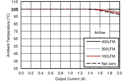
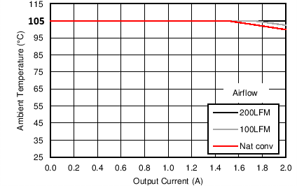
The temperature derating curves represent the conditions at which internal components are at or below the manufacturer's maximum operating temperatures. Derating limits apply to devices soldered directly to a 50 mm × 100 mm, 4-layer PCB with 2 oz. copper.
LMZ34202 24Vin_33Vo_250k_SOA.png
PVIN = 24 V VOUT = 3.3 V fSW = 250 kHz
Figure 16. Safe Operating Area
LMZ34202 24Vin_75Vo_400k_SOA.png
PVIN = 24 V VOUT = 7.5 V fSW = 400 kHz
Figure 18. Safe Operating Area
LMZ34202 24Vin_5Vo_250k_SOA.png
PVIN = 24 V VOUT = 5 V fSW = 250 kHz
Figure 17. Safe Operating Area